®
Numonyx™ StrataFlash Embedded Memory (J3-65nm)
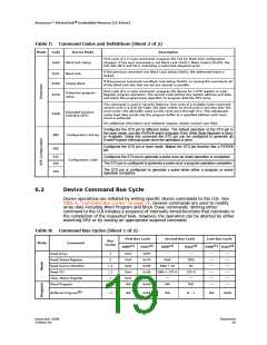
Table 7:
Command Codes and Definitions (Sheet 2 of 2)
Mode
Code
Device Mode
Description
First cycle of a 2-cycle command; prepares the CUI for block lock configuration
changes. If the next command is not Block Lock (0x01), Block Unlock (0xD0), the
CUI sets SR.5 and SR.4, indicating a command sequence error.
0x60
Block lock Setup
If the previous command was Block Lock Setup (0x60), the addressed block is
locked.
0x01
0xD0
Block lock
If the previous command was Block Lock Setup (0x60), on issuing this command, all
of the Block lock bits that are set are cleared in parallel.
Unlock Block
First cycle of a 2-cycle command; prepares the device for a OTP register or Lock
Register program operation. The second cycle latches the register address and data,
and starts the programming algorithm to program data the OTP array.
Protection program
setup
0xC0
This command is used in security features. first cycle of a multiple-cycle command
second cycle is a Sub-Op-Code, the data written on third cycle is one less than the
word count; the allowable value on this cycle are 0 through 511. The subsequent
cycles load data words into the program buffer at a specified address until word
count is achieved.
Extended Function
Interface (EFI)
0xEB
For additional information and collateral request, please contact your filed.
Configures the STS pin to different states. The default operation of the STS pin is
the level mode, just like RY/BY# which indicates if the Write State Machine is Busy
or Available. Using this command the STS pin can be configured to generate an
Erase/Program interrupt pulse once the operation is done.
B8h
00h
Configuration Set-Up
Configuration Code
Configures the STS pin in level mode. Makes the STS pin function like a RY/BY#
pin.
01h
02h
Configures the STS pin to generate a pulse once an erase operation is completed.
The STS pin is configured to generate a pulse once a program operation completes.
The STS pin is configured to generate a pulse when either a program or erase
operation completes.
03h
6.2
Device Command Bus Cycle
Device operations are initiated by writing specific device commands to the CUI. See
Table 8, “Command Bus Cycles” on page 19. Several commands are used to modify
array data including Word Program and Block Erase commands. Writing either
command to the CUI initiates a sequence of internally-timed functions that culminate in
the completion of the requested task. However, the operation can be aborted by either
asserting RP# or by issuing an appropriate suspend command.
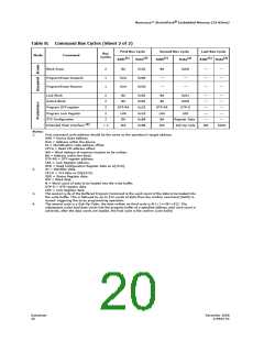
Table 8:
Command Bus Cycles (Sheet 1 of 2)
First Bus Cycle
Second Bus Cycle
Last Bus Cycle
Bus
Mode
Command
Cycles
(1)
(2)
(1)
(2)
(1)
(2)
Addr
Data
Addr
Data
Addr
Data
Read Array
1
2
DnA
DnA
DnA
DnA
DnA
WA
0xFF
---
---
SRD
ID
---
---
---
---
---
---
---
---
---
---
Read Status Register
Read Device Identifier
Read CFI
0x70
0x90
0x98
0x50
0x40
DnA
DBA + IA
DBA + CFI-A
---
≥ 2
≥ 2
1
CFI-D
---
Clear Status Register
Word Program
---
---
2
WA
WD
(3)
Buffered Program
> 2
WA
0xE8
WA
N - 1
WA
0xD0
December 2008
319942-02
Datasheet
19

 NUMONYX [ NUMONYX B.V ]