Nexperia
PBSS4260PANPS
60 V, 2 A NPN/PNP low VCEsat (BISS) double transistor
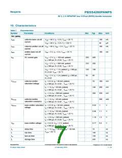
8. Limiting values
Table 5.
In accordance with the Absolute Maximum Rating System (IEC 60134).
Symbol Parameter Conditions
Limiting values
Min
Max
Unit
Per transistor, for the PNP transistor with negative polarity
VCBO
VCEO
VEBO
IC
collector-base voltage
collector-emitter voltage
emitter-base voltage
collector current
open emitter
open base
-
-
-
-
-
-
-
-
-
-
-
60
60
7
V
V
open collector
V
2
A
ICM
peak collector current
base current
single pulse; tp ≤ 1 ms
3
A
IB
0.3
1
A
IBM
peak base current
total power dissipation
single pulse; tp ≤ 1 ms
Tamb ≤ 25 °C
A
Ptot
[1]
[2]
[3]
[4]
370
570
530
700
mW
mW
mW
mW
Per device
Ptot
total power dissipation
Tamb ≤ 25 °C
[1]
[2]
[3]
[4]
-
510
780
730
960
150
150
150
mW
mW
mW
mW
°C
-
-
-
Tj
junction temperature
ambient temperature
storage temperature
-
Tamb
Tstg
-55
-65
°C
°C
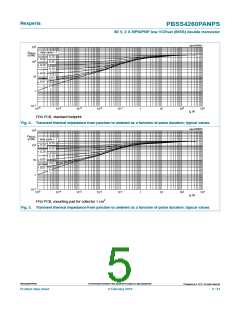
[1] Device mounted on an FR4 Printed-Circuit Board (PCB), single-sided copper, tin-plated and standard
footprint.
[2] Device mounted on an FR4 Printed-Circuit Board (PCB), single sided copper, tin-plated; mounting pad for
collector 1 cm2.
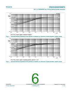
[3] Device mounted on an FR4 Printed-Circuit Board (PCB), 4-layer copper, tin-plated and standard footprint.
[4] Device mounted on an FR4 Printed-Circuit Board (PCB), 4-layer copper, tin-plated; mounting pad for
collector 1 cm2.
©
PBSS4260PANPS
All information provided in this document is subject to legal disclaimers.
Nexperia B.V. 2017. All rights reserved
Product data sheet
4 February 2016
3 / 21

 NEXPERIA [ Nexperia ]