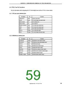
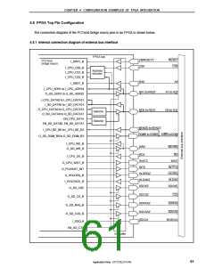
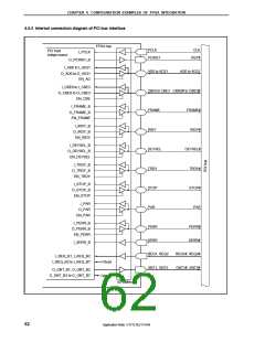
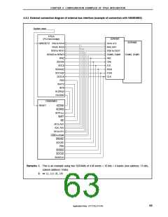
CHAPTER 4 CONFIGURATION EXAMPLES OF FPGA INTEGRATION
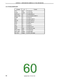
4.4.3 PCI bus interface pins
Pin Name
I/O
Input
Function
PCLK
PCI clock input
PCI reset output
PCIRST
AD0 to AD31
CBE0 to CBE3
FRAME
Output
I/O
PCI address/data I/O
PCI command/byte enable I/O
PCI frame I/O
I/O
I/O
IRDY
I/O
PCI initiator ready I/O
PCI device select I/O
PCI target ready I/O
PCI stop I/O
DEVSEL
TRDY
I/O
I/O
STOP
I/O
PAR
I/O
PCI parity I/O
PERR
I/O
PCI parity error I/O
PCI system error input
PCI request input
SERR
Input
Input
Output
Output
REQ1, REQ2
GNT1, GNT2
INT1, INT2
PCI grant output
PCI INTA, INTB output
60
Application Note U17121EJ1V1AN

 NEC [ NEC ]