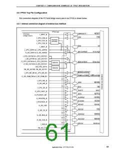
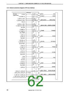
CHAPTER 4 CONFIGURATION EXAMPLES OF FPGA INTEGRATION
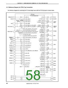
4.4 FPGA Top Pin Functions
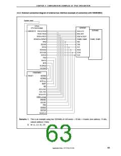
The pin information when integrating the PCI host bridge macro with an FPGA is shown below.
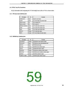
4.4.1 CPU bus slave interface pins
Pin Name
VBRESETZ
I/O
Input
Function
System reset input
CSZ6
Input
I/O
PCI host bridge chip select input
CPU address I/O
RA0 to RA25
RD0 to RD31
BENZ0 to BENZ3
WRZ
I/O
CPU data I/O
Input
Input
Input
Output
Output
CPU data byte enable input
CPU data write enable input
CPU data read enable input
CPU data wait output
RDZ
WAITZ
INT0
PCI host bridge interrupt output
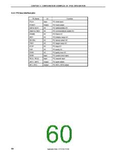
4.4.2 SDRAM bus interface pins
Pin Name
HLDREQZ
I/O
Output
Input
Function
SDRAM bus hold request output
SDRAM bus hold acknowledge input
SDRAM clock input
HLDACKZ
SDCLK
Input
SDCKE
Output
Output
Output
Output
Output
Output
SDRAM clock enable output
SDRAM chip select output
SDCS
SDRASZ
SDCASZ
SDWEZ
SDRAM row address strobe output
SDRAM column address strobe output
SDRAM read/write output
DQM0 to DQM3
SDRAM output disable output
59
Application Note U17121EJ1V1AN

 NEC [ NEC ]