CHAPTER 4 CONFIGURATION EXAMPLES OF FPGA INTEGRATION
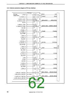
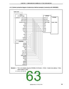
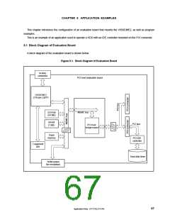
4.5.3 External connection diagram of external bus interface (example of connection with V850E/ME2)
System reset
FPGA
SDRAM1
A0 to A12
(PCI host bridge)
SDRAM2
VBRESETZ
RA2 to RA14
RA24, RA25
RD0 to RD31
BA0, BA1
DQ0 to DQ31
DQM0, DQM1
/WE
BENZ0 to BENZ3
WRZ
DQM2, DQM3
SDCKE
SDCS
CKE
/CS
SDRASZ
SDCASZ
SDCLK
RDZ
/RAS
/CAS
CLK
WAITZ
INT0
HLDRQZ
HLDAKZ
V850E/ME2
RESET
HLDAK
HLDRQ
INTPxxx
WAIT
RD
A0 to A22
A24, A25
D0 to D31
xxBE/xxDQM
WR/WE
SDCKE
CSx
SDRAS
SDCAS
BUSCLK
Remarks 1. This is an example using two SDRAMs of 4 M words × 16 bits × 4 banks (row address: 13 bits,
column address: 9 bits).
2. xx: LL, LU, UL, UU
63
Application Note U17121EJ1V1AN

 NEC [ NEC ]