CHAPTER 3 SPECIFICATIONS OF PCI HOST BRIDGE MACRO
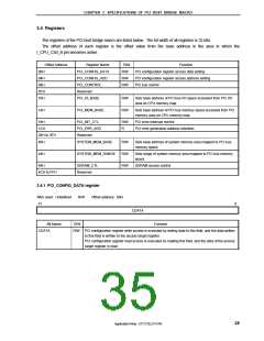
3.4 Registers
The registers of the PCI host bridge macro are listed below. The bit width of all registers is 32 bits.
The offset address of each register is the offset value from the base address in the area in which the
I_CPU_CS0_B pin becomes active.
Offset Address
Register Name
PCI_CONFIG_DATA
PCI_CONFIG_ADD
PCI_CONTROL
Reserved
R/W
R/W
Function
PCI configuration register access data setting
PCI configuration register access address setting
PCI bus control
00H
04H
08H
R/W
R/W
0CH
10H
PCI_IO_BASE
R/W
R/W
Sets base address of PCI bus I/O space accessed from PCI I/O
area on CPU memory map
14H
PCI_MEM_BASE
Sets base address of PCI bus memory space accessed from PCI
memory area on CPU memory map
18H
PCI_INT_CTL
R/W
R
PCI error interrupt control
1CH
PCI_ERR_ADD
Reserved
PCI error generation address retention
20H to 3FH
40H
SYSTEM_MEM_BASE
R/W
R/W
R/W
Sets base address of system memory area mapped to PCI bus
memory space
44H
SYSTEM_MEM_RANGE
Sets range of system memory area mapped to PCI bus memory
space
48H
SDRAM_CTL
Reserved
SDRAM access control
4CH to FFH
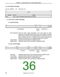
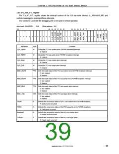
3.4.1 PCI_CONFIG_DATA register
After reset: Undefined
31
R/W
Offset address: 00H
0
CDATA
Bit Name
CDATA
R/W
Function
R/W PCI configuration register write access is executed by writing data to this field, and the data written
to this field is written to the access target register.
PCI configuration register read access is executed by reading this field, and the data of the access
target register is read.
35
Application Note U17121EJ1V1AN

 NEC [ NEC ]