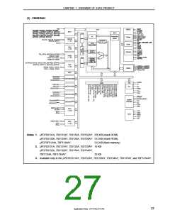
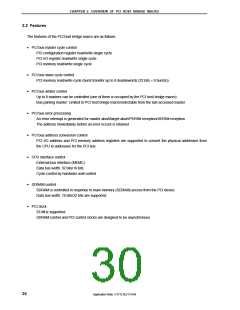
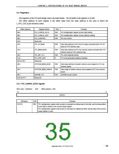
CHAPTER 3 SPECIFICATIONS OF PCI HOST BRIDGE MACRO
This chapter describes the block diagram, signals, register specifications, and operation specifications of the PCI
host bridge macro.
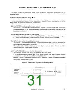
3.1 Internal Blocks of PCI Host Bridge Macro
The PCI host bridge macro consists of the four blocks shown in Figure 3-1 General Block Diagram of PCI Host
Bridge Macro. The functions of each block are described below.
(1) LM_BRIDGE: External bus interface master controller
This controller is connected to the external bus interface, responds to accesses from the CPU, and issues an
access request to the PH_FLIP_BRIDGE block of the PCI bus controller. A bus width of 16 bits or 32 bits can
be accessed from the CPU.
(2) LS_BRIDGE: External bus interface slave controller
This controller responds to accesses from the PH_FLIP_BRIDGE block of the PCI bus controller in response
to a memory data transfer request from the PCI device and issues an access request to SDRAMC.
(3) SDRAMC: External bus interface SDRAM controller
This controller is connected to the SDRAM bus. A memory request from the PCI device via the LS_BRIDGE
block is transferred by activating the SDRAM bus.
When the bus width of SDRAM is 16 bits, memory cycles of up to 8 bursts are started. When the bus width is
32 bits, memory cycles of up to 4 bursts are started.
(4) PH_FLIP_BRIDGE: External bus interface host controller
This controller is connected to the PCI bus and operates as the PCI host device.
A PCI configuration register read/write cycle, PCI IO register read/write cycle, and PCI memory read/write
cycle are started in response to a request from the LM_BRIDGE block.
Moreover, a request is issued to the LS_BRIDGE block in response to a memory data transfer request from
the PCI device connected to the PCI bus.
Figure 3-1. General Block Diagram of PCI Host Bridge Macro
PCI host bridge macro
External bus
LM_BRIDGE
interface
PCI bus
interface
PH_FLIP_BRIDGE
SDRAM bus
SDRAMC
LS_BRIDGE
interface
31
Application Note U17121EJ1V1AN

 NEC [ NEC ]