µPD703100A-33, 703100A-40, 703101A-33, 703102A-33
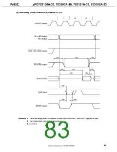
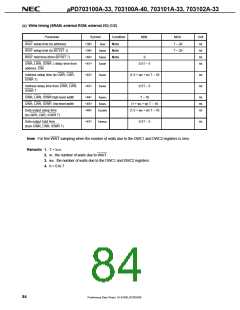
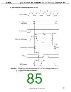
(c) Write timing (SRAM, external ROM, external I/O) (1/2)
Parameter
Symbol
<38>
Condition
Note
MIN.
MAX.
T – 20
T – 20
Unit
ns
WAIT setup time (to address)
WAIT setup time (to BCYST ↓)
WAIT hold time (from BCYST ↑)
tSAW
tSBSW
tHBSW
tDAWR
<39>
<40>
<41>
Note
ns
Note
0
ns
UWR, LWR, IOWR ↓ delay time from
0.5T – 5
ns
address, CSn
Address setup time (to UWR, LWR,
<42>
<43>
tSAWR
(1.5 + wD + w) T – 10
0.5T – 5
ns
ns
IOWR ↑)
Address delay time from UWR, LWR,
tDWRA
IOWR ↑
UWR, LWR, IOWR high-level width
UWR, LWR, IOWR low-level width
<44>
<45>
<46>
tWWRH
tWWRL
tSODWR
T – 10
ns
ns
ns
(1 + wD + w) T – 10
(1.5 + wD + w) T – 10
Data output setup time
(to UWR, LWR, IOWR ↑)
Data output hold time
<47>
tHWROD
0.5T – 5
ns
(from UWR, LWR, IOWR ↑)
Note For first WAIT sampling when the number of waits due to the DWC1 and DWC2 registers is zero.
Remarks 1. T = tCYK
2. w: the number of waits due to WAIT.
3. wD: the number of waits due to the DWC1 and DWC2 registers.
4. n = 0 to 7
84
Preliminary Data Sheet U14168EJ2V0DS00

 NEC [ NEC ]