PDF
最近搜索
热门搜索
发布采购

| 型号: | UPD703100AGJ-40-8EU |
| PDF下载: | 下载PDF文件 查看货源 |
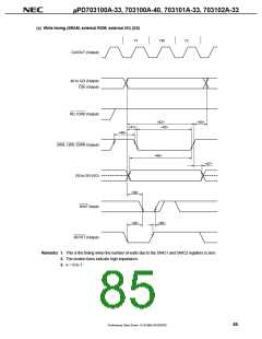
| 内容描述: | V850E / MS1TM 16分之32位单芯片微控制器 [V850E/MS1TM 32/16-BIT SINGLE-CHIP MICROCONTROLLERS] |
| 分类和应用: | 微控制器和处理器外围集成电路时钟 |
| 文件页数/大小: | 132 页 / 1155 K |
| 品牌: |  NEC [ NEC ] NEC [ NEC ] |
专业IC领域供求交易平台:提供全面的IC Datasheet资料和资讯,Datasheet 1000万数据,IC品牌1000多家。