µPD703100A-33, 703100A-40, 703101A-33, 703102A-33
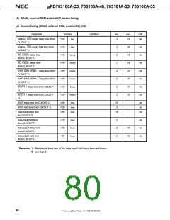
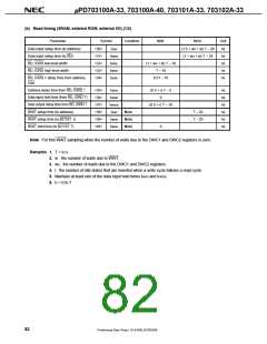
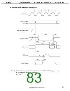
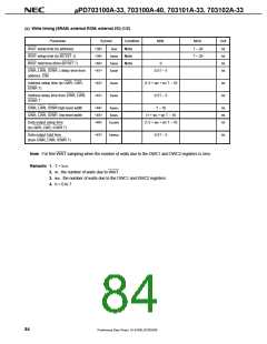
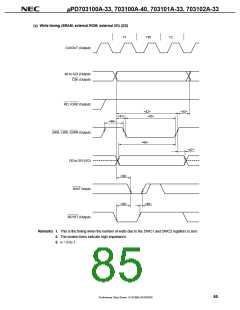
(b) Read timing (SRAM, external ROM, external I/O) (1/2)
Parameter
Symbol
<30>
Condition
MIN.
MAX.
Unit
ns
Data input setup time (to address)
Data input setup time (to RD)
RD, IORD low-level width
RD, IORD high-level width
tSAID
tSRDID
tWRDL
tWRDH
tDARD
(1.5 + wD + w) T – 20
(1 + wD + w) T – 24
<31>
<32>
<33>
<34>
ns
(1 + wD + w) T – 10
T – 10
ns
ns
RD, IORD ↓ delay time from address,
0.5T – 10
ns
CSn
Address delay time from RD, IORD ↑
<35>
<36>
<37>
<38>
<39>
<40>
tDRDA
tHRDID
tDRDOD
tSAW
(0.5 + i) T – 5
0
ns
ns
ns
ns
ns
ns
Data input hold time (from RD, IORD )
↑
Data output delay time from RD, IORD
WAIT setup time (to address)
WAIT setup time (to BCYST ↓)
WAIT hold time (to BCYST ↑)
↑
(0.5 + i) T – 10
Note
Note
Note
T – 20
T – 20
tSBSW
tHBSW
0
Note For first WAIT sampling when the number of waits due to the DWC1 and DWC2 registers is zero.
Remarks 1. T = tCYK
2. w: the number of waits due to WAIT.
3. wD: the number of waits due to the DWC1 and DWC2 registers.
4. i: the number of idle states that are inserted when a write cycle follows a read cycle.
5. Maintain at least one of the data input hold times tHKID and tHRDID.
6. n = 0 to 7
82
Preliminary Data Sheet U14168EJ2V0DS00

 NEC [ NEC ]