µPD703100A-33, 703100A-40, 703101A-33, 703102A-33
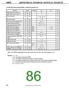
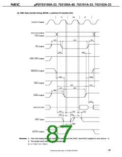
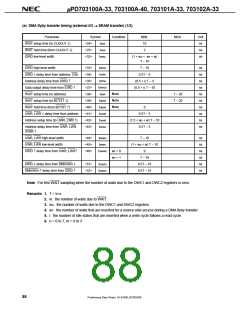
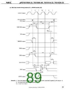
(d) DMA flyby transfer timing (SRAM → external I/O transfer) (1/2)
Parameter
Symbol
<24> tSWK
tHKW
Condition
Unit
ns
MIN.
10
2
MAX.
WAIT setup time (to CLKOUT ↓)
WAIT hold time (from CLKOUT ↓)
RD low-level width
<25>
<32>
ns
tWRDL
(1 + wD + wF + w)
T – 10
ns
RD high-level width
<33>
<34>
<35>
<37>
<38>
<39>
<40>
<41>
<42>
<43>
tWRDH
tDARD
tDRDA
tDRDOD
tSAW
T – 10
ns
ns
ns
ns
ns
ns
ns
ns
ns
ns
RD ↓ delay time from address, CSn
Address delay time from RD ↑
Data output delay time from RD ↑
WAIT setup time (to address)
WAIT setup time (to BCYST ↓)
WAIT hold time (from BCYST ↑)
IOWR ↓ delay time from address
Address setup time (to IOWR ↑)
0.5T – 5
(0.5 + i) T – 5
(0.5 + i) T – 10
Note
Note
Note
T – 20
T – 20
tSBSW
tHBSW
tDAWR
tSAWR
tDWRA
0
0.5T – 5
(1.5 + wD + w) T – 10
0.5T – 5
Address delay time from UWR, LWR,
IOWR ↑
IOWR high-level width
<44>
<45>
<48>
tWWRH
tWWRL
tDWRRD
T – 10
(1 + wD + w) T – 10
0
ns
ns
ns
ns
ns
ns
IOWR low-level width
RD ↑ delay time from IOWR ↑
wF = 0
wF = 1
T – 10
IOWR ↓ delay time from DMAAKm ↓
DMAAKm ↑ delay time from IOWR ↑
<49>
<50>
tDDAWR
tDWRDA
0.5T – 10
(0.5 + wF) T – 10
Note For first WAIT sampling when the number of waits due to the DWC1 and DWC2 registers is zero.
Remarks 1. T = tCYK
2. w: the number of waits due to WAIT.
3. wD: the number of waits due to the DWC1 and DWC2 registers.
4. wF: the number of waits that are inserted for a source-side access during a DMA flyby transfer.
5. i: the number of idle states that are inserted when a write cycle follows a read cycle.
6. n = 0 to 7, m = 0 to 3
86
Preliminary Data Sheet U14168EJ2V0DS00

 NEC [ NEC ]