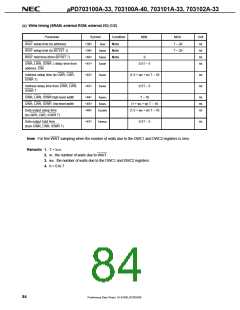
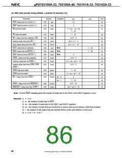
µPD703100A-33, 703100A-40, 703101A-33, 703102A-33
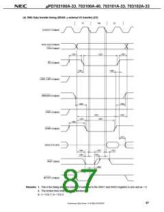
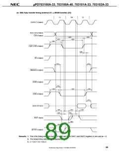
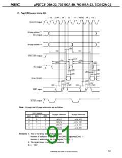
(d) DMA flyby transfer timing (SRAM → external I/O transfer) (2/2)
T1
TW
T2
CLKOUT (Output)
A0 to A23 (Output)
CSn (Output)
<33>
<32>
<35>
RD (Output)
UWR, LWR (Output)
DMAAKm (Output)
IORD (Output)
<34>
<48>
<49>
<41>
<50>
<43>
<42>
<45>
<44>
IOWR (Output)
<37>
D0 to D15 (I/O)
WAIT (Input)
<38>
<24>
<25>
<24>
<25>
<40>
<39>
BCYST (Output)
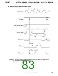
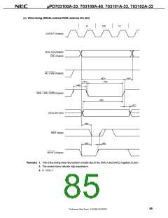
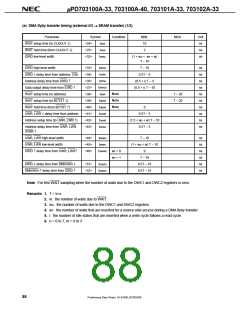
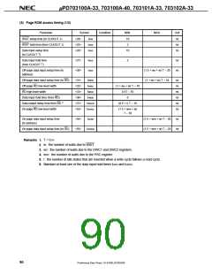
Remarks 1. This is the timing when the number of waits due to the DWC1 and DWC2 registers is zero and wF = 0.
2. The broken lines indicate high impedance.
3. n = 0 to 7, m = 0 to 3
87
Preliminary Data Sheet U14168EJ2V0DS00

 NEC [ NEC ]