µPD703100A-33, 703100A-40, 703101A-33, 703102A-33
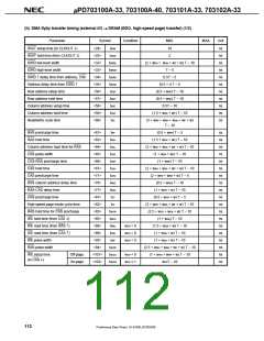
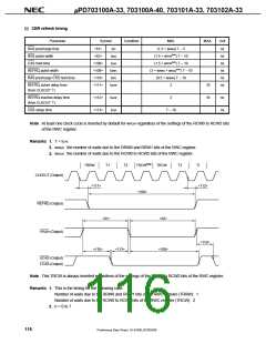
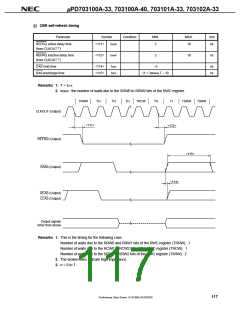
(i) CBR refresh timing
Parameter
RAS precharge time
RAS pulse width
Symbol
Condition
MIN.
(1.5 + wRRW) T – 5
(1.5 + w
MAX.
Unit
ns
ns
ns
ns
ns
ns
<61>
tRP
tRAS
RCWNote) T – 10
<62>
<108>
<109>
<110>
<111>
(1.5 + w
RCWNote) T – 10
CAS hold time
tCHR
tWRFL
tRPC
tDKRF
REFRQ pulse width
RAS precharge CAS hold time
(3 + w
RRW + wRCWNote) T – 10
(0.5 + wRRW) T – 10
2
REFRQ active delay time
10
10
(from CLKOUT ↑)
REFRQ inactive delay time
<112>
<113>
tHKRF
2
ns
ns
(from CLKOUT ↑)
CAS setup time
tCSR
T – 10
Note At least one clock cycle is inserted by default for wRCW regardless of the settings of the RCW0 to RCW2 bits
of the RWC register.
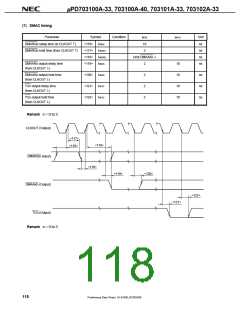
Remarks 1. T = tCYK
2. wRRW: the number of waits due to the RRW0 and RRW1 bits of the RWC register.
3. wRCW: the number of waits due to the RCW0 to RCW2 bits of the RWC register.
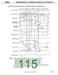
TRRW
T1
T2
TRCWNote
TRCW
T3
TI
CLKOUT (Output)
REFRQ (Output)
RASn (Output)
<111>
<112>
<109>
<61>
<62>
<110>
<110>
<113>
<108>
UCAS (Output)
LCAS (Output)
Note This TRCW is always inserted regardless of the settings of the RCW0 to RCW2 bits of the RWC register.
Remarks 1. This is the timing for the following case.
Number of waits due to the RRW0 and RRW1 bits of the RWC register (TRRW): 1
Number of waits due to the RCW0 to RCW2 bits of the RWC register (TRCW): 2
2. n = 0 to 7
116
Preliminary Data Sheet U14168EJ2V0DS00

 NEC [ NEC ]