µPD703100A-33, 703100A-40, 703101A-33, 703102A-33
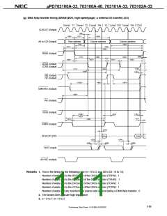
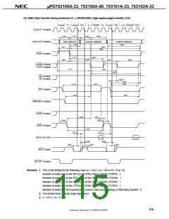
(h) DMA flyby transfer timing (external I/O → DRAM (EDO, high-speed page) transfer) (3/3)
TRPW T1 TRHW TW
T2 TDAW T3 TCPW TW
TO1 TDAW TO2
CLKOUT (Output)
A0 to A23 (Output)
RASn (Output)
<56>
<57>
<58>
<59>
Row address
<76>
<61>
Column address
Column address
<64>
<94>
<60>
<77>
<65>
<66>
<67>
<81>
<63>
UCAS (Output)
LCAS (Output)
<71>
<82>
<83>
RD (Output)
OE (Output)
<102>
<88>
<89>
<101>
<105>
<85>
WE (Output)
<92>
DMAAKm (Output)
IOWR (Output)
IORD (Output)
D0 to D15 (I/O)
WAIT (Input)
<106>
<107>
<35>
<34>
<32>
<24>
<25>
<33>
Data
Data
<24>
<24>
<25>
<25>
BCYST (Output)
Remarks 1. This is the timing for the following case (n = 0 to 3, xx = 00 to 03, 10 to 13).
Number of waits due to the RPCxx bit of the DRCn register (TRPW): 1
Number of waits due to the RHCxx bit of the DRCn register (TRHW): 1
Number of waits due to the DACxx bit of the DRCn register (TDAW): 1
Number of waits due to the CPCxx bit of the DRCn register (TCPW): 1
Number of waits that are inserted for a source-side access during a DMA flyby transfer: 0
2. The broken lines indicate high impedance.
3. n = 0 to 7, m = 0 to 3
115
Preliminary Data Sheet U14168EJ2V0DS00

 NEC [ NEC ]