CHAPTER 13 LCD CONTROLLER/DRIVER
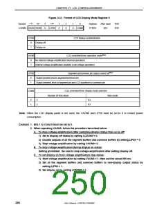
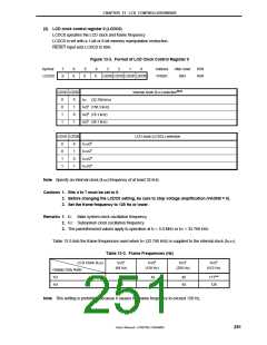
(2) LCD clock control register 0 (LCDC0)
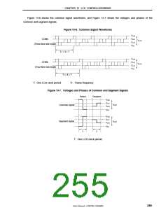
LCDC0 specifies the LCD clock and frame frequency.
LCDC0 is set with a 1-bit or 8-bit memory manipulation instruction.
RESET input sets LCDC0 to 00H.
Figure 13-3. Format of LCD Clock Control Register 0
Symbol
LCDC0
7
0
6
0
5
0
4
3
2
1
0
Address
FFB2H
After reset
00H
R/W
R/W
0
LCDC03 LCDC02 LCDC01 LCDC00
LCDC03 LCDC02
Internal clock (fLCD) selectionNote
0
0
1
1
0
1
0
1
f
f
f
f
XT
(32.768 kHz)
X
X
X
/25 (156.3 kHz)
/26 (78.1 kHz)
/27 (39.1 kHz)
LCDC01 LCDC00
LCD clock (LCDCL) selection
0
0
1
1
0
1
0
1
f
f
f
f
LCD/26
LCD/27
LCD/28
LCD/29
Note Specify an internal clock (fLCD) frequency of at least 32 kHz.
Cautions 1. Bits 4 to 7 must be set to 0.
2. Before changing the LCDC0 setting, be sure to stop voltage amplification (VAON0 = 0).
3. Set the frame frequency to 128 Hz or lower.
Remarks 1. fX: Main system clock oscillation frequency
2. fXT: Subsystem clock oscillation frequency
3. The parenthesized values apply to operation at fX = 5.0 MHz or fXT = 32.768 kHz.
Table 13-3 lists the frame frequencies used when fXT (32.768 kHz) is supplied to the internal clock (fCLK1).
Table 13-3. Frame Frequencies (Hz)
LCD Clock (fLCD)
Display Duty Ratio
fXT/29
fXT/28
fXT/27
fXT/26
(64 Hz)
(128 Hz)
(256 Hz)
(512 Hz)
1/3
1/4
21
16
43
32
85
64
171Note
128
Note This setting is prohibited because it causes the frame frequency to exceed 128 Hz.
User’s Manual U15075EJ1V0UM00
251

 NEC [ NEC ]