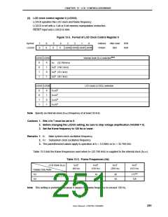
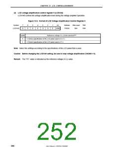
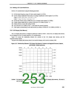
CHAPTER 13 LCD CONTROLLER/DRIVER
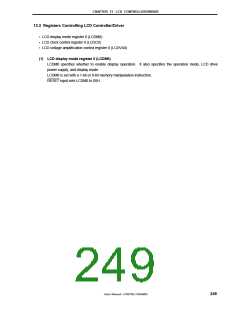
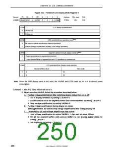
Figure 13-2. Format of LCD Display Mode Register 0
Symbol
<7> <6>
5
0
<4>
3
0
2
0
1
0
0
Address
FFB0H
After reset
00H
R/W
R/W
LCDM0 LCDON0 VAON0
LIPS0
LCDM00
LCDON0
LCD display enable/disable
0
1
Display off
Display on
VAON0
LCD controller/driver operation modeNote
0
1
No internal voltage amplification (Normal operation)
Internal voltage amplification enabled (Low-voltage operation)
LIPS0
Segment pin/common pin output control bitNote
0
1
Output ground level to segment/common pin
Output deselect level to segment pin and LCD waveform to common pin
LCD controller/driver display mode selection
Number of time slices
LCDM00
Bias mode
4
3
1/3
1/3
0
1
Note When the LCD display panel is not used, the VAON0 and LIPS0 must be set to 0 to reduce power
consumption.
Cautions 1. Bits 1 to 3 and 5 must be set to 0.
2. When operating VAON0, follow the procedure described below.
A. To stop voltage amplification after switching display status from on to off:
1) Set to display off status by setting LCDON0 = 0.
2) Disable outputs of all the segment buffers and common buffers by setting LIPS0 = 0.
3) Stop voltage amplification by setting VAON0= 0.
B. To stop voltage amplification during display on status:
Setting prohibited. Be sure to stop voltage amplification after setting display off.
C. To set display on from voltage amplification stop status:
1) Start voltage amplification by setting VAON0 = 1, then wait for about 500 ms.
2) Set all the segment buffers and common buffers to non-display output status by
setting LIPS0 = 1.
3) Set display on by setting LCDON0 = 1.
250
User’s Manual U15075EJ1V0UM00

 NEC [ NEC ]