CHAPTER 13 LCD CONTROLLER/DRIVER
13.4 Setting LCD Controller/Driver
Set the LCD controller/driver using the following procedure.
<1> Set the frame frequency using LCD clock control register 0 (LCDC0).
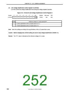
<2> Set the voltage amplification level using LCD voltage amplification control register 0 (LCDVA0).
GAIN = 0: VLC0 = 4.5 V, VLC1 = 3 V, VLC2 = 1. 5 V
GAIN = 1: VLC0 = 3 V, VLC1 = 2 V, VLC2 = 1 V
<3> Set the time division using LCDM00 (bit 0 of LCD display mode register 0 (LCDM0)).
<4> Enable voltage amplification by setting VAON0 (bit 6 of LCDM0) (VAON0 = 1).
<5> Wait for 500 ms or more after setting VAON0.
<6> Set LIPS0 (bit 4 of LCDM0) (LIPS0 = 1) and output the deselect potential.
<7> Start output corresponding to each data memory by setting LCDON0 (bit 7 of LCDM0) (LCDON0 =1).
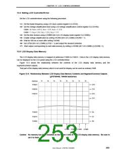
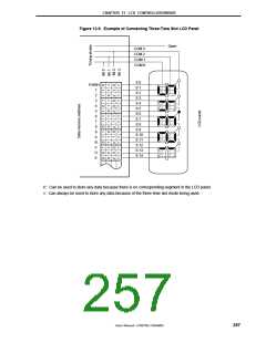
13.5 LCD Display Data Memory
The LCD display data memory is mapped at addresses FA00H to FA0EH. Data in the LCD display data memory
can be displayed on the LCD panel using the LCD controller/driver.
Figure 13-5 shows the relationship between the contents of the LCD display data memory and the
segment/common outputs.
That part of the display data memory which is not used for display can be used as ordinary RAM.
Figure 13-5. Relationship Between LCD Display Data Memory Contents and Segment/Common Outputs
(µPD789446, 789456 Subseries)
b7
b6
b5
b4
b3
b2
b1
b0
Address
FA0EH
S14
S13
S12
S11
FA0DH
FA0CH
FA02H
FA01H
FA00H
S2
S1
S0
COM3 COM2 COM1 COM0
Caution No memory has been installed as the higher 4 bits of the LCD display data memory. Be sure to
set 0 to them.
User’s Manual U15075EJ1V0UM00
253

 NEC [ NEC ]