CHAPTER 13 LCD CONTROLLER/DRIVER
13.6 Common and Segment Signals
Each pixel of the LCD panel turns on when the potential difference between the corresponding common and
segment signals becomes higher than a specific voltage (LCD drive voltage, VLCD). It turns off when the potential
difference becomes lower than VLCD.
Applying DC voltage to the common and segment signals for an LCD panel would deteriorate it. To avoid this
problem, this LCD panel is driven with AC voltage.
(1) Common signals
Each common signal is selected sequentially according to a specified number of time slots at the timing
listed in Table 13-4. In the static display mode, the same signal is output to COM0 to COM3 in common.
In the three-time slot mode, keep the COM3 pin open.
Table 13-4. COM Signals
COM Signal
COM0
COM1
COM2
COM3
Number of Time Slots
Three-time slot mode
Four-time slot mode
Open
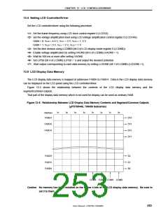
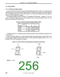
(2) Segment signals
The segment signals correspond to LCD display data memory. Bits 0, 1, 2, and 3 of each byte are read in
synchronization with COM0, COM1, COM2, and COM3, respectively. If the contents of each bit are 1, it is
converted to the select voltage, and if 0, it is converted to the deselect voltage. The conversion results are
output to the segment pins.
Check, with the information given above, what combination of the front-surface electrodes (corresponding to
the segment signals) and the rear-surface electrodes (corresponding to the common signals) forms display
patterns in the LCD display data memory, and write the bit data that corresponds to the desired display
pattern on a one-to-one basis.
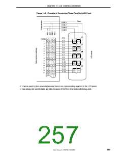
Bit 3 of the LCD display data memory is not used for LCD display in the three-time slot mode. So this bit
can be used for purposes other than display.
LCD display data memory bits 4 to 7 are fixed to 0.
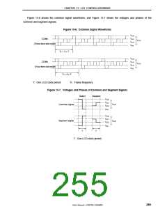
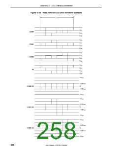
(3) Output waveforms of common and segment signals
Voltages listed in Table 13-5 are output as common and segment signals.
When both common and segment signals are at the select voltage, a display-on voltage of ±VLCD is
obtained. The other combinations of the signals correspond to the display-off voltage.
Table 13-5. LCD Drive Voltage
Segment Signal
Select Signal Level
VSS0/VLC0
Deselect Signal Level
Common Signal
VLC1/VLC2
VLCD
1
3
1
3
1
Select signal level
VLC0/VSS0
VLC2/VLC1
–VLCD/+VLCD
–
–
VLCD/+
3
1
3
1
3
1
3
Deselect signal level
–
VLCD/+
VLCD
VLCD/+
VLCD
254
User’s Manual U15075EJ1V0UM00

 NEC [ NEC ]