NB675 –24V, HIGH CURRENT SYNCHRONOUS BUCK CONVERTER
pin and SW pin. GND is used as the positive
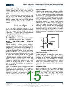
UVLO Protection
current sensing node so that GND should be
connected to the source terminal of the bottom
MOSFET.
The NB675 has under-voltage lock-out protection
(UVLO). When the VCC voltage is higher than
the UVLO rising threshold voltage, the part will
be powered up. It shuts off when the VIN voltage
is lower than the UVLO falling threshold voltage.
This is non-latch protection. The part is disabled
when the VCC voltage falls below 4.5V. If an
application requires a higher under-voltage
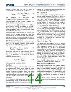
lockout (UVLO), use the EN pin as shown in
Figure 9 to adjust the input voltage UVLO by
using two external resistors. It is recommended
to use the enable resistors to set the UVLO
falling threshold (VSTOP) above 4.5V. The rising
threshold (VSTART) should be set to provide
enough hysteresis to allow for any input supply
variations.
Since the comparison is done during the high
side MOSFET OFF and low side MOSFET ON
state, the OC trip level sets the valley level of the
inductor current. Thus, the load current at over-
current threshold, IOC, can be calculated as
follows:
ΔI
inductor
IOC = I_limit +
(13)
2
In an over-current condition, the current to the
load exceeds the current to the output capacitor;
thus the output voltage tends to fall off.
Eventually, it will end up with crossing the under
voltage protection threshold and shutdown.
VTT Over-Current Protection
IN
NB675
The VTT LDO has an internally fixed current limit
of 1.8A for source operation, and 1.6A for sink.
RUP
EN Comparator
VDDQ
Over/Under-Voltage
Protection
(OVP/UVP)
EN
NB675 monitors a resistor divided feedback
voltage to detect over and under voltage. When
the feedback voltage becomes higher than 115%
of the target voltage, the controller will enter
Dynamic Regulation Period. During this period,
the LS will off when the LS current goes to -1A,
this will then discharge the output and try to keep
it within the normal range. If the dynamic
regulation can not limit the increasing of the Vo,
once the feedback voltage becomes higher than
130% of the feedback voltage, the OVP
comparator output goes high and the circuit
latches as the high-side MOSFET driver OFF
and the low-side MOSFET turn on acting as an -
1A current source.
RDOWN
Figure 9—Adjustable UVLO
Thermal Shutdown
Thermal shutdown is employed in the NB675.
The junction temperature of the IC is internally
monitored. If the junction temperature exceeds
the threshold value (typical 150ºC), the converter
shuts off. This is a non-latch protection. There is
about 25ºC hysteresis. Once the junction
temperature drops to about 125ºC, it initiates a
SS.
Output Discharge
When the feedback voltage becomes lower than
60% of the target voltage, the UVP comparator
output goes high if the UV still occurs after 26us
delay; then the fault latch will be triggered---
latches HS off and LS on; the LS FET keeps on
until the inductor current goes zero.
NB675 discharges all the outputs, including
VDDQ, VTTREF and VTT when EN2=low, or the
controller is turned off by the protection functions
(UVP & OCP, OCP, OVP, UVLO, and thermal
shutdown). The part discharge the outputs using
an internal 6ꢀ MOSFET.
NB675 Rev. 1.0
1/14/2013
www.MonolithicPower.com
MPS Proprietary Information. Patent Protected. Unauthorized Photocopy and Duplication Prohibited.
© 2013 MPS. All Rights Reserved.
15

 MPS [ MONOLITHIC POWER SYSTEMS ]