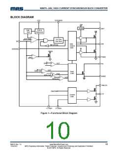
NB675 –24V, HIGH CURRENT SYNCHRONOUS BUCK CONVERTER
resistor (RDOWN from EN pin to GND) to
determine the automatic start-up voltage:
voltage on the internal reference exceeds the
sensed output voltage at the FB node.
VTT and VTTREF
RUP + R
V
= 1.45×
DOWN (V)
(9)
IN−START
This part integrates two high performance, low-
drop-out linear regulators, VTT and VTTREF, to
provide complete DDR3/DDR3L power solutions.
The VTTREF has a 10-mA sink/source current
capability, and track 1/2 of VDDQSEN using an
on-chip divider. A minimum 0.22μF ceramic
capacitor must be connected close to the
VTTREF terminal for stable operation.
RDOWN
For
example,
for
RUP=150kΩ
and
RDOWN=51kΩ,the VIN−START is set at 5.52V.
To avoid noise, a 10nF ceramic capacitor from
EN to GND is recommended.
There is an internal Zener diode on the EN pin,
which clamps the EN pin voltage to prevent it
from running away. The maximum pull up current
assuming a worst case 12V internal Zener clamp
should be less than 1mA.
The VTT regulator responses quickly to track
VTTREF with +/-45mV under all conditions. The
current capability of the VTT regulator is up to
1.5A for both sink and source modes. A minimum
10μF ceramic capacitor need to be connected
close to the VTT terminal. The VTTSEN should
be connected to the positive node of VTT output
capacitor as a separated trace from the high-
current line to the VTT pin.
Therefore, when EN is driven by an external logic
signal, the EN voltage should be lower than
12V.when EN is connected with VIN through a
pull-up resistor or a resistive voltage divider, the
resistance selection should ensure the maximum
pull up current less than 1mA.
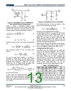
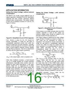
VDDQ Power Good (PG)
If using a resistive voltage divider and VIN higher
than 12V, the allowed minimum pull-up resistor
The NB675 has power-good (PGOOD) output
used to indicate whether the output voltage of the
VDDQ regulator is ready or not. The PGOOD pin
is the open drain of a MOSFET. It should be
connected to VCC or other voltage source through
a resistor (e.g. 100k,). After the input voltage is
applied, the MOSFET is turned on so that the
PGOOD pin is pulled to GND before SS is ready.
After FB voltage reaches 95% of REF voltage,
the PGOOD pin is pulled high after a delay. The
PGOOD delay time is 1ms.
RUP should meet the following equation:
V (V)−12
RUP(kΩ)
12
IN
(10)
−
< 1(m A )
RDOWN(kΩ)
Especially, just using the pull-up resistor RUP (the
pull-down resistor is not connected), the
V
IN-START is determined by input UVLO, and the
minimum resistor value is:
V (V) −12
IN
(11)
RUP(kΩ) >
When the FB voltage drops to 85% of REF
voltage, the PGOOD pin will be pulled low.
1(m A )
A typical pull-up resistor is 100kꢀ.
VDDQ Over Current Protection
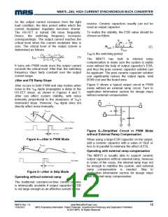
Soft Start
NB675 has cycle-by-cycle over current limiting
control. The current-limit circuit employs a
"valley" current-sensing algorithm. The part use
the Rds(on) of the low side MOSFET as a
current-sensing element. If the magnitude of the
current-sense signal is above the current-limit
threshold, the PWM is not allowed to initiate a
new cycle.
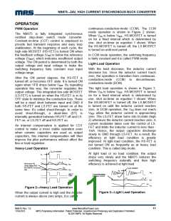
The NB675 employs soft start (SS) mechanism
to ensure smooth output during power-up. When
the EN pin becomes high, the internal reference
voltage ramps up gradually; hence, the output
voltage ramps up smoothly, as well. Once the
reference voltage reaches the target value, the
soft start finishes and it enters into steady state
operation.
The trip level is fixed internally. The inductor
current is monitored by the voltage between GND
If the output is pre-biased to a certain voltage
during startup, the IC will disable the switching of
both high-side and low-side switches until the
NB675 Rev. 1.0
1/14/2013
www.MonolithicPower.com
MPS Proprietary Information. Patent Protected. Unauthorized Photocopy and Duplication Prohibited.
© 2013 MPS. All Rights Reserved.
14

 MPS [ MONOLITHIC POWER SYSTEMS ]