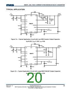
NB675 –24V, HIGH CURRENT SYNCHRONOUS BUCK CONVERTER
APPLICATION INFORMATION
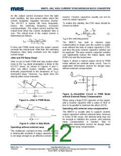
Setting the Output Voltage---without external
compensation
Setting the Output Voltage ―with external
compensation
The NB675 can usually support different type of
output capacitors, including POSCAP, electrolytic
capacitor and also ceramic capacitors without
external ramp compensation, The output voltage
is then set by feedback resistors R1 and R2. As
Figure 10 shows.
SW
L
Vo
R4
R1
R2
FB
C4
R9
Ceramic
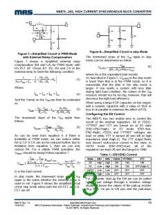
SW
L
Vo
Figure11—Simplified Circuit of Ceramic
Capacitor
C4
R1
R2
FB
If the system is not stable enough when low ESR
ceramic capacitor is used in the output, an
external voltage ramp should be added to FB
through resistor R4 and capacitor C4.
CAP
The output voltage is influenced by ramp voltage
VRAMP besides R divider as shown in Figure 11.
The VRAMP can be calculated as shown in
equation 7. R2 should be chosen reasonably, a
small R2 will lead to considerable quiescent
current loss while too large R2 makes the FB
noise sensitive. It is recommended to choose a
Figure10—Simplified Circuit of POS Capacitor
First, choose a value for R2. R2 should be
chosen reasonably, a small R2 will lead to
considerable quiescent current loss while too
large R2 makes the FB noise sensitive. Typically,
set the current through R2 at around 5-10uA will
make a good balance between system stability
and also the no load loss. Then R1 is determined
as follow with the output ripple considered:
1
value within 5kꢀ-50kꢀ for R2, using
a
comparatively larger R2 when Vo is low,
etc.,1.05V, and a smaller R2 when Vo is high.
And the value of R1 then is determined as follow:
VOUT
−
ΔVOUT − VREF
R2
2
(14)
(13)
R1 =
⋅R2
R1=
V
VREF
R2
FB(AVG)
-
(VOUT -VFB(AVG) ) R4 +R9
ΔVOUT is the output ripple, refer to equation (23)
The VFB(AVG) is the average value on the FB,
VFB(AVG) varies with the Vin, Vo, and load
condition, etc., its value on the skip mode would
be lower than that of the PWM mode, which
means the load regulation is strictly related to the
Other than feedback resistors, a feed forward
cap C4 is usually applied for a better transient
performance, especially when ceramic caps are
applied for their small capacitance, a cap value
around 100pF-1nF is suggested for a better
transient while also keep the system stable with
enough noise immunity. In case the system is
noise sensitive because of the zero induced by
this cap, add a resistor-usually named as R9
between this cap and FB to form a pole, this
resistor can be set according to equation (16) as
in the following section.
V
V
FB(AVG). Also the line regulation is related to the
FB(AVG). If one wants to gets a better load or line
regulation, a lower Vramp is suggested, as long
as the criterion shown in equation 8 can be met.
For PWM operation, VFB(AVG) value can be
deduced from the equation below.
1
R1 //R2
V
= VREF + VRAMP
×
(15)
FB(AVG)
2
R1 //R2 +R9
NB675 Rev. 1.0
1/14/2013
www.MonolithicPower.com
MPS Proprietary Information. Patent Protected. Unauthorized Photocopy and Duplication Prohibited.
© 2013 MPS. All Rights Reserved.
16

 MPS [ MONOLITHIC POWER SYSTEMS ]