NB675 –24V, HIGH CURRENT SYNCHRONOUS BUCK CONVERTER
Usually, R9 is set to 0ꢀ, and it can also be set
X7R ceramic dielectrics are recommended
because they are fairly stable with temperature
fluctuations.
following equation 16 for a better noise immunity.
It should also set to be 5 times smaller than
R1//R2 to minimize its influence on Vramp.
The capacitors must also have a ripple current
rating greater than the maximum input ripple
current of the converter. The input ripple current
can be estimated as follows:
1
R9 =
(16)
2π×C4 ×2F
SW
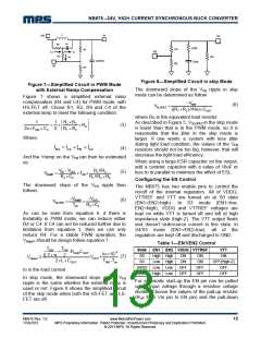
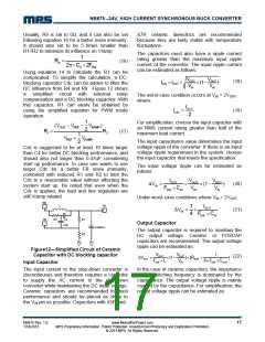
Using equation 14 to calculate the R1 can be
complicated. To simplify the calculation, a DC-
blocking capacitor Cdc can be added to filter the
DC influence from R4 and R9. Figure 12 shows
VOUT
VOUT
(18)
ICIN = IOUT
×
×(1−
)
V
V
IN
IN
a
simplified circuit with external ramp
The worst-case condition occurs at VIN = 2VOUT
where:
,
compensation and a DC-blocking capacitor. With
this capacitor, R1 can easily be obtained by
using the simplified equation for PWM mode
operation:
IOUT
ICIN
=
(19)
2
1
For simplification, choose the input capacitor with
an RMS current rating greater than half of the
maximum load current.
(VOUT − VREF − VRAMP
)
2
R1 =
R2
(17)
1
VREF + VRAMP
The input capacitance value determines the input
voltage ripple of the converter. If there is an input
voltage ripple requirement in the system, choose
the input capacitor that meets the specification.
2
Cdc is suggested to be at least 10 times larger
than C4 for better DC blocking performance, and
should also not larger than 0.47uF considering
start up performance. In case one wants to use
larger Cdc for a better FB noise immunity,
combined with reduced R1 and R2 to limit the
Cdc in a reasonable value without affecting the
system start up. Be noted that even when the
Cdc is applied, the load and line regulation are
still Vramp related.
The input voltage ripple can be estimated as
follows:
IOUT
SW ×CIN
VOUT
VOUT
ΔV =
×
×(1−
)
(20)
IN
F
V
V
IN
IN
Under worst-case conditions where VIN = 2VOUT
:
SW
L
Vo
IOUT
4 FSW ×CIN
1
ΔV =
×
(21)
IN
FB
R4
R1
R2
C4
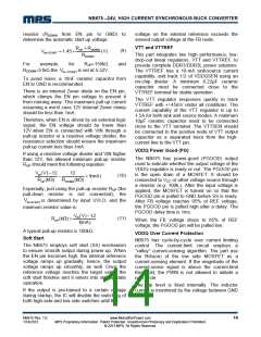
Output Capacitor
Cdc
Ceramic
The output capacitor is required to maintain the
DC output voltage. Ceramic or POSCAP
capacitors are recommended. The output voltage
ripple can be estimated as:
Figure12—Simplified Circuit of Ceramic
Capacitor with DC blocking capacitor
VOUT
V
1
(22)
)
ΔVOUT
=
×(1− OUT )×(RESR
+
FSW ×L
V
8×FSW ×COUT
IN
Input Capacitor
The input current to the step-down converter is
discontinuous and therefore requires a capacitor
to supply the AC current to the step-down
converter while maintaining the DC input voltage.
Ceramic capacitors are recommended for best
performance and should be placed as close to
the VIN pin as possible. Capacitors with X5R and
In the case of ceramic capacitors, the impedance
at the switching frequency is dominated by the
capacitance. The output voltage ripple is mainly
caused by the capacitance. For simplification, the
output voltage ripple can be estimated as:
NB675 Rev. 1.0
1/14/2013
www.MonolithicPower.com
MPS Proprietary Information. Patent Protected. Unauthorized Photocopy and Duplication Prohibited.
© 2013 MPS. All Rights Reserved.
17

 MPS [ MONOLITHIC POWER SYSTEMS ]