NB675 –24V, HIGH CURRENT SYNCHRONOUS BUCK CONVERTER
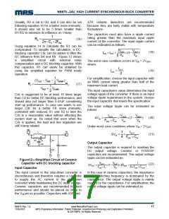
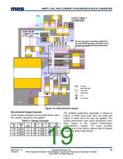
PGND
DO NOT CONNECT
TO PGND HERE
To
AGND
VOUT
AGND KELVIN
CONNECT TO PGND
AT VCC CAP
AGND
At least two layers should be applied for
Vin and PGND and place >20 vias close to
the part for a better thermal performance
LP
FB
14
EN2
17
VCC
16
EN1
15
PG
13
18
VIN
12
BST
SW
1
2
3
VIN
19
20
21
VIN
PGND
PGND
11
10
PGND
9
4
5
6
7
8
AGND
--Top Layer
--Inner PGND Layer
--Inner Layer2
--Bottom Layer
--Via
--Via For AGND
VOUT
PGND
Figure 13—Recommend Layout
Recommend Design Example
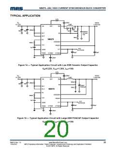
The detailed application schematic is shown in
Figure 14 when large ESR caps are used and
Figure 15 when low ESR caps are applied. The
typical performance and circuit waveforms have
been shown in the Typical Performance
Characteristics section. For more possible
applications of this device, please refer to related
Evaluation Board Data Sheets.
Some design examples are provided below when
the ceramic capacitors are applied:
Table 2—Design Example
VOUT
(V)
Cout
(F)
L
(μH)
R4
(Ω)
C4
(F)
R1
(kΩ)
R2
(kΩ)
1.05
1.2
22μx3
22μx3
22μx3
1.2
1.2
1.2
NS
NS
NS
220p
220p
220p
59
82
102
82
100
100
1.35
NB675 Rev. 1.0
1/14/2013
www.MonolithicPower.com
MPS Proprietary Information. Patent Protected. Unauthorized Photocopy and Duplication Prohibited.
© 2013 MPS. All Rights Reserved.
19

 MPS [ MONOLITHIC POWER SYSTEMS ]