NB675 –24V, HIGH CURRENT SYNCHRONOUS BUCK CONVERTER
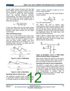
L
Vo
SW
Vo
C4
R4
ESR
R1
R1
IR4
IC4
FB
R9
IFB
Ro
Ceramic
Cout
R2
FB
R2
Figure 8—Simplified Circuit in skip Mode
Figure 7—Simplified Circuit in PWM Mode
with External Ramp Compensation
The downward slope of the VFB ripple in skip
mode can be determined as follow:
Figure 7 shows a simplified external ramp
compensation (R4 and C4) for PWM mode, with
HS-FET off. Chose R1, R2, R9 and C4 of the
external ramp to meet the following condition:
−VREF
(8)
VSLOPE2
=
( R +R //Ro)×C
(
)
1
2
OUT
where Ro is the equivalent load resistor.
⎛
⎜
⎝
⎞
⎟
⎠
R1 ×R2
R1 + R2
1
1
5
As described in Figure 5, VSLOPE2 in the skip mode
is lower than that is in the PWM mode, so it is
reasonable that the jitter in the skip mode is
larger. If one wants a system with less jitter
during light load condition, the values of the VFB
resistors should not be too big, however, that will
decrease the light load efficiency.
<
×
+ R9
(3)
2π×FSW × C4
Where:
IR4 = IC4 +IFB ≈ IC4
(4)
And the Vramp on the VFB can then be estimated
as:
When using a large-ESR capacitor on the output,
add a ceramic capacitor with a value of 10uF or
less to in parallel to minimize the effect of ESL.
V − VOUT
R4 ×C4
R1 //R2
IN
(5)
VRAMP
=
×TON ×
R1 //R2 +R9
Configuring the EN Control
The downward slope of the VFB ripple then
follows
The NB675 has two enable pins to control the
on/off of the internal regulators. All of VDDQ,
VTTREF and VTT are turned on at S0 state
(EN1=EN2=high). In S3 mode (EN1=low,
EN2=high), VDDQ and VTTREF voltages are
kept on while VTT is turned off and left at high
impedance state (high-Z). The VTT output floats
and doesn’t sink/source current in this state. In
S4/S5 mode (EN1=EN2=low), all of the
regulators are kept off and discharged to GND.
−VRAMP
−VOUT
R4 ×C4
(6)
VSLOPE1
=
=
T
off
As can be seen from equation 6, if there is
instability in PWM mode, we can reduce either
R4 or C4. If C4 can not be reduced further due to
limitation from equation 3, then we can only
reduce R4. For a stable PWM operation, the
Vslope1 should be design follow equation 7.
Table 1—EN1/EN2 Control
TSW
T
ON -RESRCOUT
State
S0
EN1 EN2 VDDQ VTTREF
VTT
ON
+
Io×10-3
TSW -Ton
0.7×π
2
High High
Low High
ON
ON
ON
ON
(7)
-Vslope1
≥
VOUT +
2×L×COUT
S3
OFF(High-Z)
OFF
S4/S5 Low Low
Others High Low
OFF
OFF
OFF
OFF
Io is the load current.
OFF
In skip mode, the downward slope of the VFB
ripple is the same whether the external ramp is
used or not. Figure 8 shows the simplified circuit
of the skip mode when both the HS-FET and LS-
FET are off.
For automatic start-up the EN pin can be pulled
up to input voltage through a resistive voltage
divider. Choose the values of the pull-up resistor
(RUP from Vin pin to EN pin) and the pull-down
NB675 Rev. 1.0
1/14/2013
www.MonolithicPower.com
MPS Proprietary Information. Patent Protected. Unauthorized Photocopy and Duplication Prohibited.
© 2013 MPS. All Rights Reserved.
13

 MPS [ MONOLITHIC POWER SYSTEMS ]