PDF
最近搜索
热门搜索
发布采购

| 型号: | NB675 |
| PDF下载: | 下载PDF文件 查看货源 |
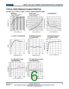
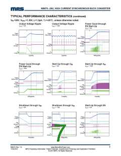
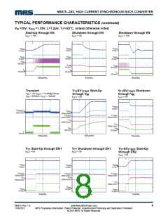
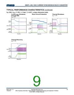
| 内容描述: | 24V高电流同步降压转换器1.5A LDO和磨光参考 [24V, High Current Synchronous Buck Converter With 1.5A LDO and Buffed Reference] |
| 分类和应用: | 转换器 |
| 文件页数/大小: | 21 页 / 617 K |
| 品牌: |  MPS [ MONOLITHIC POWER SYSTEMS ] MPS [ MONOLITHIC POWER SYSTEMS ] |
专业IC领域供求交易平台:提供全面的IC Datasheet资料和资讯,Datasheet 1000万数据,IC品牌1000多家。