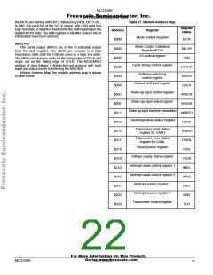
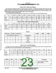
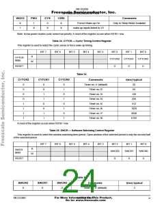
FreesScPaI RlEeGISSTMeERCmS33Di3cE8S9oCRnIPdTuIOcNtor, Inc.
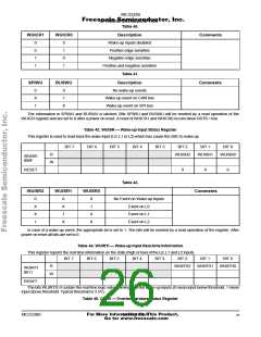
Table 40.
WUICR1
WUICR0
Description
Comments
Comments
0
0
1
1
0
1
0
1
Wake-up inputs disabled
Positive edge sensitive
Negative edge sensitive
Positive and negative sensitive
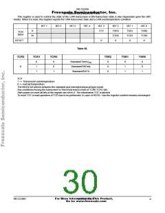
Table 41.
SPIWU
BUSWU
Description
0
X
1
0
1
No wake-up events
Wake-up event on CAN bus
Wake-up event on SPI bus
X
The information in SPIWU and BUSWU is latched. Bits SPIWU and BUSWU will be reseted by a read operation of the
WUICR register and are set to 0 after a power on reset. A reset of WUICR1 and WUICR0 occurs when RSTB = low.
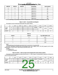
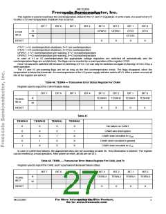
Table 42. WUISR — Wake-up Input Status Register
This register is used to read back the wake input (L0, L1 or L2) which has cause the SBC to wake up.
BIT 7
BIT 6
BIT 5
BIT 4
BIT 3
BIT 2
BIT 1
BIT 0
R
WUISR2
WUISR1
WUISR0
WUISR
$00F
W
RESET
0
0
0
Table 43.
WUISR2
WUISR1
WUISR0
Comments
0
X
X
1
0
X
1
0
1
No Event on Wake-up Inputs
Event on L0
X
X
Event on L1
X
Event on L2
In case of a wake-up event, the appropriate bit is set to 1. The bits will be reseted by a read operation of the register. After
power on reset all bits are set to 0.
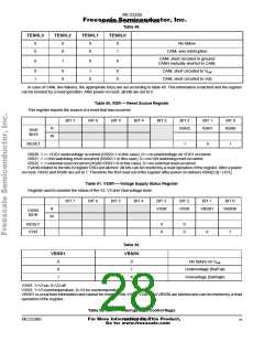
Table 44. WUIRTI — Wake-up Input Real-time Information
This register reports the real time information on the state (high or low) of the L0, L1 and L2 inputs.
BIT 7
BIT 6
BIT 5
BIT 4
BIT 3
BIT 2
BIT 1
BIT 0
R
WUIRTI2
WUIRTI1
WUIRTI0
WUIRTI
$011
W
RESET
The bits WUIRTI2-0 contain the real time logic value coming from the wake-up inputs (0 mean input below threshold, 1 mean
input above threshold. Typical threshold is 3.5V).
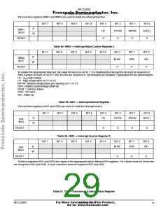
Table 45. OTSR — Overtemperature Status Register
For More Information On This Product,
MC33389
MOTOROLA
26
Go to: www.freescale.com

 MOTOROLA [ MOTOROLA ]