MC33389
Freescale Semiconductor, Inc.
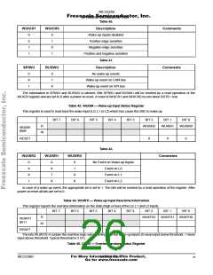
SPI REGISTER DESCRIPTION
the MOSI pin starting with Bit15, followed by Bit14, Bit13, etc.,
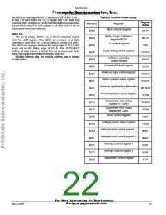
Table 27. Module Address Map
to Bit0. For each fall of the SCLK signal, with CSB held in a
logic low state, a databit is loaded into the shift register per the
databit MOSI state.The shift register is full after sixteen bits of
information have been entered.
Register
Name
Address
$000
$003
$005
$006
$009
$00A
$00C
$00F
$011
$012
$014
$017
$018
$01B
$01D
$01E
$021
$022
$024
Register
Mode Control Register
MCR
MCVR
V3R
MISO Pin
Mode Control Validation
RegisterMCVR
The serial output (MISO) pin is the tri-stateable output
from the shift register. The MISO pin remains in a high
impedance state until the CSB pin goes to a logic low state.
The MISO pin changes state on the rising edge of SCLK and
reads out on the falling edge of SCLK. The MOSI/MISO
shifting of data follows a first-in-first-out protocol with both
input and output words transferring the MSB first.
Module Address Map, the module address map is shown
in table below.
V3 control register
Cyclic timing control register
CYTCR
SWCR
GSLR
WUICR
WUISR
WUIRTI
OTSR
TESRH
TESRL
RSR
Software watchdog
control register
Ground shift level register
Wake-up input control register
Wake-up input status register
Wake up input real time information
Overtemperature status register
Transceiver error status
register for CANH
Transceiver error status
register for CANL
Reset source register
Voltage supply status register
Interrupt mask control register 1
Interrupt mask control register 2
Interrupt source register 1
Interrupt source register 2
Transceiver control register
VSSR
IMR1
IMR2
ISR1
ISR2
TCR
For More Information On This Product,
Go to: www.freescale.com
MC33389
MOTOROLA
22

 MOTOROLA [ MOTOROLA ]