FreesScPaI RlEeGISSTMeERCmS33Di3cE8S9oCRnIPdTuIOcNtor, Inc.
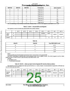
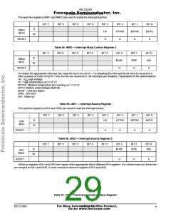
The next two registers (IMR1 and IMR2) are used to mask the interrupt function.
BIT 7
BIT 6
BIT 5
BIT 4
BIT 3
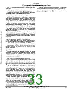
HV
0
BIT 2
HTPW
0
BIT 1
MTPW
0
BIT 0
BATU
0
R
IMR1
$01D
W
RESET
Table 54. IMR2 — Interrupt Mask Control Register 2
BIT 6 BIT 5 BIT 4 BIT 3
BIT 7
BIT 2
BUSF
0
BIT 1
SPIE
0
BIT 0
WU
0
R
IMR2
$01E
W
RESET
To enable the appropriate interrupt, the mask bit has to be set to 1. For disabling the interrupt the bit must be cleared to 0.
After a power on reset or RSTB = low, the bits are cleared to 0. All interrupts are disabled. Explanation for the abbreviations:
HV : Vbat high voltage
HT : High temperature on V1 or V2
MTPW : Medium temperature pre-warning on V1 or V2
BATU: Battery undervoltage (BatFail)
BUSF : CAN bus failure
SPIE : SPI error
WU : Wake-up
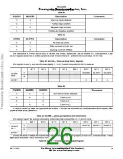
Table 55. ISR1 — Interrupt Source Register
The next two registers (ISR1 and ISR2) are used to read the interrupt source.
BIT 7
BIT 6
BIT 5
BIT 4
BIT 3
HV
BIT 2
BIT 1
BIT 0
R
HTPW
MTPW
BATU
ISR
$021
W
RESET
0
0
0
0
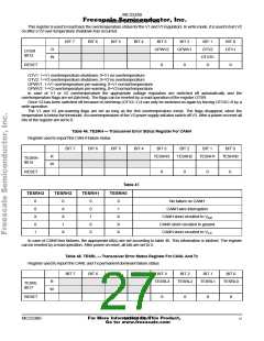
Table 56. ISR2 — Interrupt Source Register 2
BIT 6 BIT 5 BIT 4 BIT 3
BIT 7
BIT 2
BIT 1
SPIE
BIT 0
WU
R
BUSF
ISR
$022
W
RESET
0
0
0
All bits in registers ISR1 and ISR2 are copies of the appropriate bits in different SPI registers. For a faster read out, these bits
are merged in ISR1 and ISR2. A reset cannot be done for registers ISR1 and ISR2.
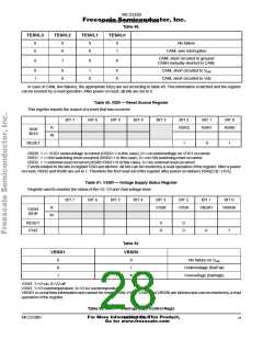
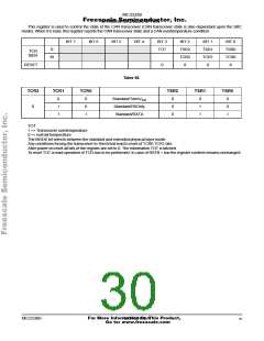
Table 57. TCR—Transceiver Control/Status Register
For More Information On This Product,
MC33389
MOTOROLA
29
Go to: www.freescale.com

 MOTOROLA [ MOTOROLA ]