MC33389
Freescale Semiconductor, Inc.
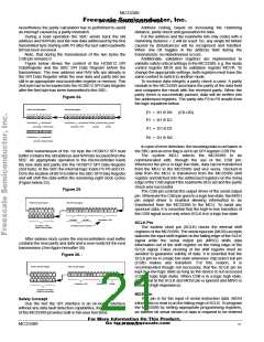
DEVICE DESCRIPTION
WAKE-UP CAPABILITIES
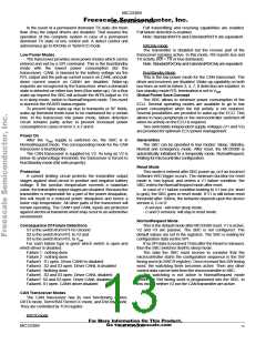
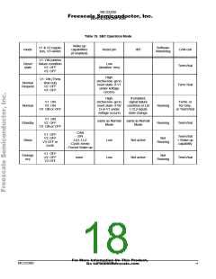
SBC Modes
Local Wake-up Behaviour
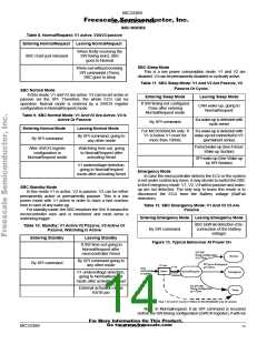
Detection Principle
Detection active according to the option.
The event is stored in WUISR register.The
SBC may activate INTB output.
The gnd shift to detect is selected via the SPI out of 4
different values (-0.7V, -1.2V, -1.7V, -2.2V). At each TX falling
edge (end of recessive state) CANH voltage is sensed. If it is
detected to be below the selected gnd shift threshold, the bit
SHIFT is set at 1 in GSLR register. No filter is implemented.
Required filtering for reliable detection should be done by
software (e.g. several trials).
Normal and
Standby
Real time state of each wake-up input
pin available in WUIRTI register
Detection active according to the option.
The event is stored in WUISR register. The
SBC switches to NormalRequest mode
Sleep
Emergency
No detection
DEVICE DIFFERENT VERSIONS
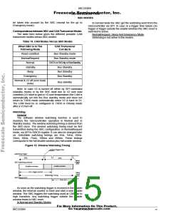
Wake-up By SPI
In some applications, the microcontroller might be
supplied by an external VDD and remains powered in SBC
Sleep mode. In this case, a feature is provided which makes
possible to wake-up the SBC by SPI activity.
The MC33389 is proposed in several package versions,
and also offers slight differences in term of functionalities.
The device version is identified in the device part number
by the first letter after the 389 number.
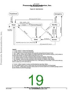
After V1 is totally switched off in sleep mode (V1<1.5V), if
a falling edge occurs on CSB (crossing 2.5V threshold), a
wake-up by SPI is detected, the SBC switches to
NormalRequest mode. A flag is set in ISR2.
The package identification is done by the last two letters of
the part number (DW for SO28 wide body, DH for power
SO20).
Interrupt Output
The INTB output may be activated in the following cases:
• Vbat overvoltage (BatHigh)
Differences between A, C and D versions:
• Vbat undervoltage (BatFail)
Behavior for V1 low:
• High temperature on V1 or V2
• Pre-warning temperature on V1 or V2
• CAN bus failure
A version:
If V1 is below reset threshold, device enters reset mode,
and if V1 stays below reset threshold for more than 100ms,
then the SBC automatically enters sleep mode. This could be
the case if V1 is shorted or permanently over loaded, and
going to sleep mode would then avoid system over current
consumption.
• SPI error
• Local wake-up (can be used for low battery detection)
• Bus wake-up
All these interrupts are maskable (See Register
Description Section).
This concerns the device reference: MC33389ADW and
MC33389ADH.
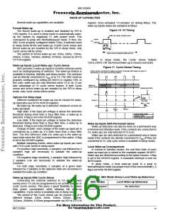
RSTB Input/Output
C and D versions:
The RSTB (reset) pin is an input/output pin. The typical
reset duration from SBC to microcontroller is 1ms. If longer
times are required, an external capacitor can be used. SBC
provides two RSTB output pull-up currents.
If V1 is below reset threshold, the SBC enters and stays in
reset mode (reset low) permanently.
This concerns the device reference: MC33389CDW and
MC33389CDH and MC33389DDW
A typical 30µA pull up when Vreset is below 2.5V and a
300uA pull up when reset voltage is higher than 2.5V.
RSTB is also an input for the SBC. It means the MC33389
is forced to NormalRequest mode after RSTB is released by
the microcontroller
Reset threshold specification:
A and C versions:
The reset threshold is defined per table “electrical
parameter, V1 pin 5V.
This concerns device MC33389ADW, ADH, CDW and
CDH
GND SHIFT DETECTION
D version : The reset threshold for the D version is slightly
higher than the A and C versions. Refer to device electrical
parameter table, V1 pin 5V
General
This concerns device reference MC33389DDW.
When normally working in two-wire operating mode, the
CAN transmission can afford some ground shift between
different nodes without trouble. Nevertheless, in case of bus
failure, the transceiver switches to single-wire operation,
therefore working with less noise margin. The affordable
ground shift is decreased in this case.
The SBC is provided with a ground shift detection for
diagnosis purpose. Four ground shift levels are selectable
and the detection is stored in the GSLR register which is
accessible via the SPI.
For More Information On This Product,
Go to: www.freescale.com
MC33389
MOTOROLA
17

 MOTOROLA [ MOTOROLA ]