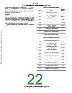
MC33389
Freescale Semiconductor, Inc.
SPI FUNCTIONNAL DESCRIPTION
nevertheless the parity calculation has to performed to avoid
Address coding, based on increasing the Hamming
an interrupt caused by a parity mismatch.
distance, parity check and generation for data.
During a read operation the SBC sends back the old
address and R/W bits and the new data addressed by the first
transmitted byte starting with P3 after the last valid read/write
bit has been received.
For the address and the read/write bits only codes with a
Hamming distance < 2 will be used. So, any single bit failure
caused by disturbances will be recognized and handled.
When one bit toggles in the address field during the
transmission, no misbehaviour occurs.
Note, that during the transmission of the two bytes the
CSB pin remains 0.
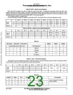
Additionally, validation registers are implemented to
validate safety critical settings in the MC33389, e.g. the mode
control register MCR and its validation register MCVR. To
change the appropriate settings, both registers must have the
same content to switch to another mode.
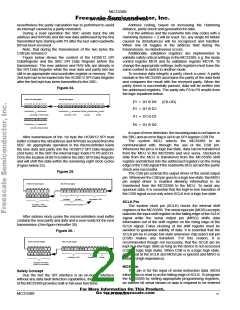
Figure below shows the content of the HC08/12 SPI
DataRegister and the SBC SPI Data Register before the
transmission. The new address and R/W bits are already in
the SPI Data Register while the new data and parity bits are
still in an appropriate microcontroller register or memory. This
2nd byte has to be loaded into the HC08/12 SPI Data Register
after the first byte has been transmitted to the SBC.
To increase data integrity a parity check is used. A parity
module in the MC33389 ascertains the parity of the data field
and compares the result with the received parity. When the
parity check is successfully passed, data will be written into
the addressed registers. The parity bits P3 to P0 results from
the logic equations below:
Figure 24.
HC08/12 SPI Data Register
SBC SPI Data Register
P3 = D3 ⊕ D0
P2 = D3 ⊕ D2
(EX-OR)
Bit7 Bit6 Bit5 Bit4 Bit3 Bit2 Bit1 Bit0
Bit15 Bit14 Bit13 Bit12 Bit11 Bit10 Bit9 Bit8 Bit7 Bit6 Bit5 Bit4 Bit3 Bit2 Bit1 Bit0
A5 A4 A3 A2 A1 A0 RW RW P3 P2 P1 P0 D3 D2 D1 D0
A5 A4 A3 A2 A1 A0
0
0
new address + R/W (1st byte)
old address + R/W
old parity
old data
P1 = D2 ⊕ D1
P0 = D1 ⊕ D0
0
0
0
0
0
0
0
0
new data + parity (2nd byte)
In case of error detection, the incoming data is not taken in
the SBC and an error flag is set in an SPI register.CSB Pin
The system MCU selects the MC33389 to be
communicated with, through the use of the CSB pin.
Whenever the pin is in logic low state, data can be transferred
from the MCU to the MC33389 and vice versa. Clocked-in
data from the MCU is transferred from the MC33389 shift
register and latched into the addressed registers on the rising
edge of the CSB signal if the read/write bit is set and the parity
check was successful.
After transmission of the 1st byte the HC08/12 SPI read
buffer contains the old address and R/W bits received from the
SBC. An appropriate operation in the microcontroller loads
the new data and parity into the HC08/12 SPI Data Register
(2nd byte). In the SBC the internal logic loads P3-P0 and D3-
D0 to the location of Bit15 to Bit8 in the SBC SPI Data Register
and will shift this data within the remaining eight clock cycles
(Figure below 25).
Figure 25.
The CSB pin controls the output driver of the serial output
pin. Whenever the CSB pin goes to a logic low state, the MISO
pin output driver is enabled allowing information to be
transferred from the MC33389 to the MCU. To avoid any
spurious data, it is essential that the high-to-low transition of
the CSB signal occur only when SCLK is in a logic low state.
HC08/12 SPI Data Register
SBC SPI Data Register
Bit7 Bit6 Bit5 Bit4 Bit3 Bit2 Bit1 Bit0
Bit15 Bit14 Bit13 Bit12 Bit11 Bit10 Bit9 Bit8 Bit7 Bit6 Bit5 Bit4 Bit3 Bit2 Bit1 Bit0
0
0
0
0
0
0
0
0
P3 P2 P1 P0 D3 D2 D1 D0 A5 A4 A3 A2 A1 A0
0
0
Bit7 Bit6 Bit5 Bit4 Bit3 Bit2 Bit1 Bit0
A5 A4 A3 A2 A1 A0 RW RW
new parity
new data
new address + R/W
SCLK Pin
old address + R/W in
HC08/12 SPI read buffer
addressed by the new address
The system clock pin (SCLK) clocks the internal shift
registers of the MC33389. The serial input pin (MOSI) accepts
data into the input shift register on the falling edge of the SCLK
signal while the serial output pin (MISO) shifts data
information out of the shift register on the rising edge of the
SCLK signal. False clocking of the shift register must be
avoided to guarantee validity of data. It is essential that the
SCLK pin be in a logic low state whenever chip select bar pin
(CSB) makes any transition. For this reason, it is
recommended though not necessary, that the SCLK pin be
kept in a low logic state as long as the device is not accessed
(CSB in logic high state). When CSB is in a logic high state,
any signal at the SCLK and MOSI pin is ignored and MISO is
tristated (high impedance).
After sixteen clock cycles the microcontrollers read buffer
contains the new parity and data and is now ready for the next
transmission (See figure hereafter 26)
Figure 26. .
HC08/12 SPI Data Register
SBC SPI Data Register
Bit7 Bit6 Bit5 Bit4 Bit3 Bit2 Bit1 Bit0
Bit15 Bit14 Bit13 Bit12 Bit11 Bit10 Bit9 Bit8 Bit7 Bit6 Bit5 Bit4 Bit3 Bit2 Bit1 Bit0
A5 A4 A3 A2 A1 A0
0
0
A5 A4 A3 A2 A1 A0 RW RW
old address + R/W
0
0
0
0
0
0
0
0
Bit7 Bit6 Bit5 Bit4 Bit3 Bit2 Bit1 Bit0
P3 P2 P1 P0 D3 D2 D1 D0
old parity
old data
new parity + new data in
HC08/12 SPI read buffer
MOSI Pin
This pin is for the input of serial instruction data. MOSI
information is read in on the falling edge of SCLK. To program
the MC33389 by setting appropriate programming registers,
an sixteen bit serial stream of data is required to be entered
Safety Concept
Due the fact the SPI interface is an on-board interface
without any data fault detection capabilities, the SPI interface
of the MC33389 provides built-in fail save functions.
For More Information On This Product,
Go to: www.freescale.com
MC33389
MOTOROLA
21

 MOTOROLA [ MOTOROLA ]