MC33389
Freescale Semiconductor, Inc.
SPI FUNCTIONNAL DESCRIPTION
General Description
Data Transfer
The SPI system is flexible enough to communicate directly
with numerous standard peripherals and MCUs available from
Motorola and other semiconductor manufacturers. SPI
reduces the number of pins necessary for input/output on the
MC33389. The SPI system of communication consists of the
MCU transmitting, and in return, receiving one databit of
information per clock cycle. Databits of information are
simultaneously transmitted by one pin, Microcontroller Out
Serial In (MOSI), and received by another pin, Microcontroller
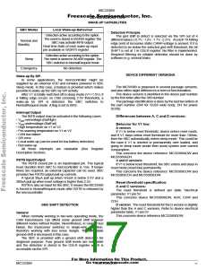
In Serial Out (MISO), of the MCU. Figure 21 below shows the
basic SPI configuration between an MCU and one MC33389.
The SPI serial operation is guaranteed to 2.0 MHz.
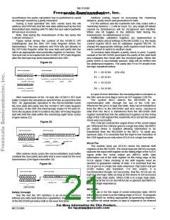
The data to and from the MC33389 are transferred in form
of two bytes.The structure of the transferred information is the
same for control the MC33389 and status reporting. The
address field A5 to A0 (Bit15 to Bit10) contains the address of
a control or status register in the MC33389. RW (Bit9 and Bit8)
contains the read/write flag for the data field. The parity field is
located at P3 to P0 (Bit7 to Bit4). The data field D3 to D0 (Bit3
to Bit0) is attached to the 2 byte data word, see figure below.
Figure 22.
Bit15 Bit14 Bit13 Bit12 Bit11 Bit10 Bit9 Bit8 Bit7 Bit6 Bit5 Bit4 Bit3 Bit2 Bit1 Bit0
MOSI
MISO
A5 A4 A3 A2 A1 A0 RW RW P3 P2 P1 P0 D3 D2 D1 D0
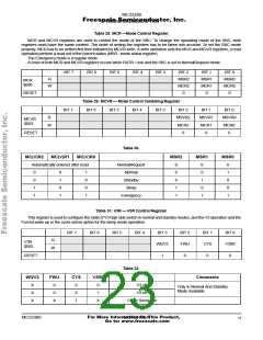
Figure 21. SPI Interface With Microcontroller
address + R/W
parity
data
MOSI
MISO
MOSI
MISO
MC68HCXX
MC33389
The SBC is accessible via the SPI interface in
NormalRequest mode, Normal mode and Standby mode. In
all other modes (Sleep mode, Emergency mode), the voltage
supply for the microcontroller in permanently switched off and
the SBC input logic for MISO, MOSI, CSB and SCLK isn’t
working (except SPI wake-up function in Sleep mode).
SCLK
CSB
Writing Data
To write data in a SPI register, two one-byte transmissions
have to performed. The first byte contains the address of the
register (MSB first) and the read/write bits which have to be
set to 1. The second byte contains the new data addressed by
the previous byte (MSB first) and the parity information. The
calculation of the parity field P3-P0 has to follow the equations
below:
Control and Status Reporting of the MC33389
The MCU is responsible for the control data transfer to the
MC33389, while the MC33389 reports its status to the MCU.
Summarized below are the major data for control and status
reporting.
- SPI initialization during start up
P3 = D3 ⊕ D0
P2 = D3 ⊕ D2
P1 = D2 ⊕ D1
P0 = D1 ⊕ D0
(EX-OR)
- MC33389 control during operation
- Watchdog triggering
- Reading status registers of the MC33389
Control Data
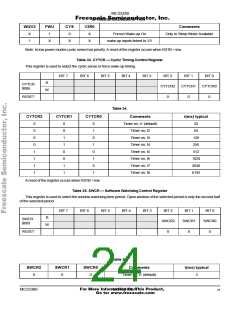
Note, that during the transmission of the two bytes the
CSB pin remains 0. See figure23 hereafter.
The control data are transferred from the MCU to the
MC33389. A control word includes an address of a certain
control register and the appropriate data. Basically the
following data will be transferred (See the SPI Register
Description section on page 21).
- MC33389 mode control
Figure 23.
HC08/12 SPI Data Register
SBC SPI Data Register
Bit7 Bit6 Bit5 Bit4 Bit3 Bit2 Bit1 Bit0
Bit15 Bit14 Bit13 Bit12 Bit11 Bit10 Bit9 Bit8 Bit7 Bit6 Bit5 Bit4 Bit3 Bit2 Bit1 Bit0
A5 A4 A3 A2 A1 A0 RW RW P3 P2 P1 P0 D3 D2 D1 D0
A5 A4 A3 A2 A1 A0
1
1
- Supply control
- Forced wake-up timing
new address + R/W (1st byte)
old address + R/W
old parity
old data
- Cyclic sense control
- Watchdog control
P3 P2 P1 P0 D3 D2 D1 D0
- Transceiver control
new data + parity (2nd byte)
Status Data
The status data are transmitted from the MC33389 to the
MCU. After receiving a valid register address from the MCU,
the MC33389 returns the appropriate status. Some of the
major status data are listed below:
- Current operation mode status
- Wake-up sources
The SBC sends back the old address, R/W, parity, and
data information from a previous transmission. This data
contains no useful information (e.g. status).It shouldn’t be used.
In case of a wrong address field or parity mismatch, an
interrupt will be issued and the SBC retains the old state.
- Reset status
Reading Data
- Error status
To read data from a dedicated register two one-byte
transmissions have to be performed. The first byte contains
the address of the register (MSB first) and the read/write flag
setting to 0. The second byte needn’t to contain valid data,
- Overtemperature status
- Transceiver status
For More Information On This Product,
Go to: www.freescale.com
MC33389
MOTOROLA
20

 MOTOROLA [ MOTOROLA ]