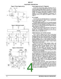
MC1377
APPLICATION INFORMATION
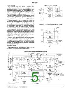
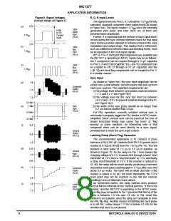
Figure 8. Signal Voltages
(Circuit Values of Figure 7)
R, G, B Input Levels
The signal levels into Pins 3, 4, 5 should be 1.0 V for fully
pp
saturated, standard composite video output levels as shown
4.4V
(a)
(b)
in Figure 9(d). The inputs require 1.0 V since the internally
generated sync pulse and color burst are at fixed and
predetermined amplitudes.
pp
100%
Green
Input
Limits
for DC
Coupled
Inputs
1.0V
1.0V
pp
(Pin 4)
Further, it is essential that the portion of each input which
occurs during the sync interval represent black for that input
since that level will be clamped to reference black in the color
modulators and output stage. This implies that a refinement,
such as a difference between black and blanking levels, must
be incorporated in the RGB input signals.
If Y, R–Y, B–Y and burst flag components are available and
the MC1377 is operating in NTSC, inputs may be as follows:
the Y component can be coupled through a 15 pF capacitor
to Pins 3, 4 and 5 tied together; the (–[R–Y]) component can
be coupled to Pin 12 through a 0.1 µF capacitor, and the
(–[B–Y]) and burst flag components can be coupled to Pin 11
in a similar manner.
2.2V
100%
Red
Input
(Pin 3)
pp
(c)
(d)
100%
Blue
Input
(Pin 5)
1.0V
pp
Sync Input
As shown in Figure 9(e), the sync input amplitude can be
varied over a wide latitude, but will require bias pull–up from
most sync sources. The important requirements are:
1)The voltage level between sync pulses must be between
1.7 V and 8.2 V, see Figure 9(e).
5.0
4.0
Composite
Output
(Pin 9)
2)The voltage level for the sync tips must be between
+0.9 V and – 0.5 V, to prevent substrate leakage in the IC,
see Figure 9(e).
3)The width of the sync pulse should be no longer than
5.2 µs and no shorter than 2.5 µs.
For PAL operation, correctly serrated vertical sync is
necessary to properly trigger the PAL divider. In NTSC mode,
simplified “block” vertical sync can be used but the loss of
proper horizontal timing may cause “top hook” or “flag
waving” in some monitors. An interesting note is that
composite video can be used directly as a sync signal,
provided that it meets the sync input criteria.
3.0
8.2 Max
1.7 Min
(e)
(f)
Sync
Input
(Pin 2)
0.9 Max
0
–0.5 Min
10.5
Chroma
Output
(Pin 13)
10.0
9.5
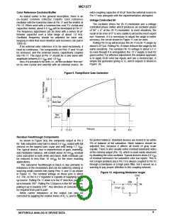
Latching Ramp (Burst Flag) Generator
The recommended application is to connect a close
tolerance (5%) 0.001 µF capacitor from Pin 1 to ground and a
resistor of 51 kΩ or 56 kΩ from Pin 1 to V (Pin 16). This will
B
(g)
4.35
4.0
produce a burst pulse of 2.5 µs to 3.5 µs in duration, as
shown in Figure 10. As the ramp on Pin 1 rises toward the
charging voltage of 8.2 V, it passes first through a burst “start
threshold” at 1.0 V, then a “stop threshold” at 1.3 V, and finally
a ramp reset threshold at 5.0 V. If the resistor is reduced to
43 kΩ, the ramp will rise more quickly, producing a narrower
and earlier burst pulse (starting approx. 0.4 µs after sync and
about 0.6 µs wide). The burst will be wider and later if the
resistor is raised to 62 kΩ, but more importantly, the 5.0 V
reset point may not be reached in one full line interval,
resulting in loss of alternate burst pulses.
As mentioned earlier, the ramp method does produce
burst at full line intervals on the “vertical porches.” If this is not
desired, and the MC1377 is operating in the NTSC mode,
burst flag may be applied to Pin 1 provided that the tip of the
pulse is between 1.0 Vdc and 1.3 Vdc. In PAL mode this
method is not suitable, since the ramp isn’t available to drive
the PAL flip–flop. Another means of inhibiting the burst pulse
is to set Pin 1 either above 1.3 Vdc or below 1.0 Vdc for the
duration that burst is not desired.
Chroma
Input
(Pin 10)
3.65
(h)
(i)
5.2
Luminance
Output
(Pin 6)
4.3
2.6
Luminance
Input
(Pin 8)
2.1
8
MOTOROLA ANALOG IC DEVICE DATA

 MOTOROLA [ MOTOROLA ]