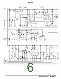
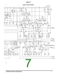
MC1377
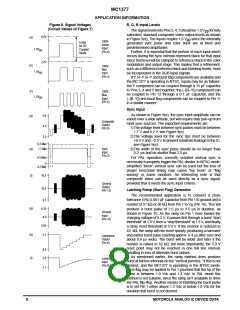
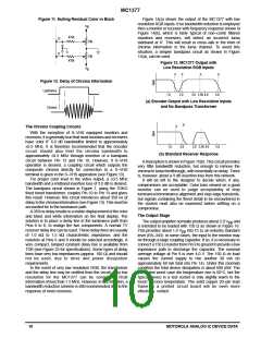
Figure 11. Nulling Residual Color in Black
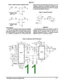
Figure 14(a) shows the output of the MC1377 with low
resolution RGB inputs. If no bandwidth reduction is employed
then a monitor or receiver with frequency response shown in
Figure 14(b), which is fairly typical of non–comb filtered
monitors and receivers, will detect an incorrect luma
sideband at X′. This will result in cross–talk in the form of
chroma information in the luma channel. To avoid this
situation, a simpler bandpass circuit as shown in Figure
15(a), can be used.
V
B
470k
470k
12
11
10k
10k
Figure 13. MC1377 Output with
Low Resolution RGB Inputs
V
B
X
X
X
X
Figure 12. Delay of Chroma Information
Luminance
1.0
2.0
3.0 3.58 4.0
5.0
(a) Encoder Output with Low Resolution Inputs
and No Bandpass Transformer
Chroma
X′
X
The Chroma Coupling Circuits
With the exception of S–VHS equipped monitors and
receivers, it is generally true that most monitors and receivers
have color IF 6.0 dB bandwidths limited to approximately
±0.5 MHz. It is therefore recommended that the encoder
circuit should also limit the chroma bandwidth to
approximately ±0.5 MHz through insertion of a bandpass
circuit between Pin 13 and Pin 10. However, if S–VHS
operation is desired, a coupling circuit which outputs the
composite chroma directly for connection to a S–VHS
terminal is given in the S–VHS application (see Figure 19).
For proper color level in the video output, a ±0.5 MHz
bandwidth and a midband insertion loss of 3.0 dB is desired.
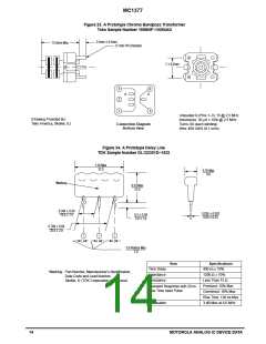
The bandpass circuit shown in Figure 7, using the TOKO
fixed tuned transformer, couples Pin 10 to Pin 13 and gives
this result. However, this circuit introduces about 350 ns of
delay to the chroma information (see Figure 13). This must be
accounted for in the luminance path.
1.0
2.0
3.0 3.58 4.0
5.0
(b) Standard Receiver Response
A final option is shown in Figure 15(b). This circuit provides
very little bandwidth reduction, but enough to remove the
chroma to luma feedthrough, with essentially no delay. There
is, however, about a 9 dB insertion loss from this network.
It will be left to the designer to decide which, if any,
compromises are acceptable. Color bars viewed on a good
monitor can be used to judge acceptability of step
luminance/chrominance alignment and step edge transients,
but signals containing the finest detail to be encountered in
the system must also be examined before settling on a
compromise.
A 350 ns delay results in a visible displacement of the color
and black and white information on the final display. The
solution is to place a delay line in the luminance path from
Pins 6 to 8, to realign the two components. A normal TV
receiver delay line can be used. These delay lines are usually
of 1.0 kΩ to 1.5 kΩ characteristic impedance, and the
resistors at Pins 6 and 8 should be selected accordingly. A
very compact, lumped constant delay line is available from
TDK (see Figure 25 for specifications). Some types of delay
lines have very low impedances (approx. 100 Ω) and should
not be used, due to drive and power dissipation
requirements.
In the event of very low resolution RGB, the transformer
and the delay line may be omitted from the circuit. Very low
resolution for the MC1377 can be considered RGB
information of less than 1.5 MHz. However, in this situation, a
bandwidth reduction scheme is still recommended due to the
response of most receivers.
The Output Stage
The output amplifier normally produces about 2.0 V and
pp
is intended to be loaded with 150 Ω as shown in Figure 16.
This provides about 1.0 V into 75 Ω, an industry standard
pp
level (RS–343). In some cases, the input to the monitor may
be through a large coupling capacitor. If so, it is necessary to
connect a 150 Ω resistor from Pin 9 to ground to provide a low
impedance path to discharge the capacitor. The nominal
average voltage at Pin 9 is over 4.0 V. The 150 Ω dc load
causes the current supply to rise another 30 mA (to
approximately 60 mA total into Pin 14). Under this (normal)
condition the total device dissipation is about 600 mW. The
calculated worst case die temperature rise is 60°C, but the
typical device in a test socket is only slightly warm to the
touch at room temperature. The solid copper 20–pin lead
frame in a printed circuit board will be even more
effectively cooled.
10
MOTOROLA ANALOG IC DEVICE DATA

 MOTOROLA [ MOTOROLA ]