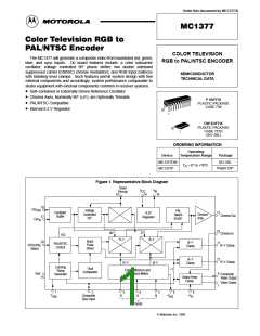
MC1377
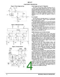
Timing Circuitry
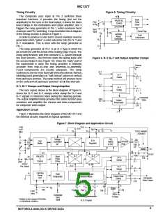
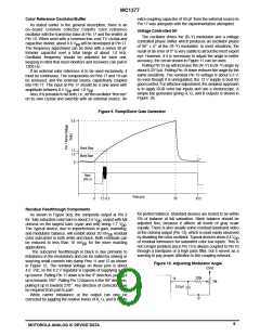
Figure 5. Timing Circuitry
The composite sync input at Pin 2 performs three
important functions: it provides the timing (but not the
amplitude) for the sync in the final output; it drives the black
level clamps in the modulators and output amplifier; and it
triggers the ramp generator at Pin 1, which produces burst
envelope and PAL switching. A representative block diagram
of the timing circuitry is shown in Figure 5.
In order to produce a color burst, a burst envelope must be
generated which “gates” a color subcarrier into the R–Y and
B–Y modulators. This is done with the ramp generator at
Pin 1.
H/2
Burst
Pulse
Driver
PAL/NTSC
Control
PAL/
NTSC
20
2
Line Drive
Sync
Input
Burst Flag
10k
V
B
Latching
Ramp
Generator
Dual
Comparator
R
1
C
The ramp generator at Pin 1 is an R–C type in which the
pin is held low until the arrival of the leading edge of sync. The
rising ramp function, with time constant R–C, passes through
two level sensors – the first one starts the gating pulse and
the second stops it (see Figure 10). Since the “early” part of
the exponential is used, the timing provided is relatively
accurate from chip–to–chip and assembly–to–assembly.
Fixed components are usually adequate. The ramp
continues to rise for more than half of the line interval, thereby
inhibiting burst generation on “half interval” pulses on vertical
front and back porches. The ramp method will produce burst
on the vertical front and back “porches” at full line intervals.
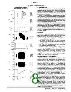
Figure 6. R–Y, B–Y and Output Amplifier Clamps
Chroma
10
B–Y
11
B–Y
Clamp
0.1
R–Y
R–Y, B–Y Clamps and Output Clamp/Amplifier
12
R–Y
Clamp
The sync signal, shown in the block diagram of Figure 6,
drives the R–Y and B–Y clamps which clamp the R–Y and
B–Y signals to reference black during the blanking periods.
The output amplifier/clamp provides this same function plus
combines and amplifies the chroma and luma components
for composite video output.
0.1
9
7
Composite
Video
Sync
Output
Amp/Clamp
0.01
8
Application Circuit
–Y
Figure 7 illustrates the block diagram of the MC1377 and
the external circuitry required for typical operation.
Figure 7. Block Diagram and Application Circuit
V
3.58/
4.43*
MHz
CC
0.01
V
B
0.1
19
14
16
TOKO 166NNF
–10264AG
17
Voltage
Controlled
PAL
Switch
0/180°
13
220
8.2V
Regulator
Osc/
Buffer
Chroma
Amp
220
90°
100/
62*
18
220
0.1
10
11
90°
0°
H/2
47/33*
1000
0.1
R–Y
B–Y
B–Y
PAL/NTS
C
Control
Burst
Pulse
Driver
20
B–Y
Clamp
3.3k
5.0 to
25pF
NTSC/
R–Y
12
PAL Select
R–Y
Clamp
0.1
Latching
Ramp
Gen
15
9
7
Dual
Comparator
Color Difference and
Luminance Matrix
Output Amp/
Clamp
Composite
Video Output
0.01
–Y
6
–Y
8
1
2
3
F
+
+
+
4
5
F
V
B
56k
1.0k
15µ
15
µF
15µ
1.0k
0.001
mica
400ns
Y Delay
R
G
B
Composite
Sync
Input
* Refers to the choice NTSC/PAL
* (3.58 MHz/4.43 MHz).
R, G, B Inputs
5
MOTOROLA ANALOG IC DEVICE DATA

 MOTOROLA [ MOTOROLA ]