MC1377
FUNCTIONAL DESCRIPTION
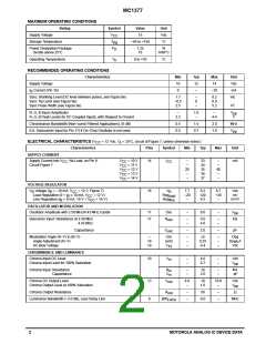
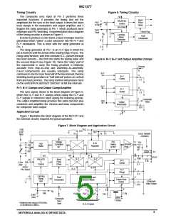
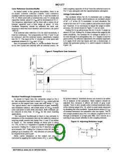
Figure 2. Power Supply and V
Power Supply and V (8.2 V Regulator)
B
B
The MC1377 pin for power supply connection is Pin 14.
From the supply voltage applied to this pin, the IC biases
internal output stages and is used to power the 8.2 V internal
0.1
V
= +12V
CC
14
16
regulator (V at Pin 16) which biases the majority of internal
B
circuitry. The regulator will provide a nominal 8.2 V and is
capable of 10 mA before degradation of performance. An
equivalent circuit of the supply and regulator is shown in
Figure 2.
100
8.2V
Regulator
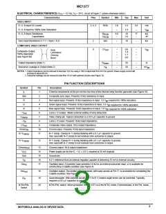
R, G, B Inputs
9
The RGB inputs are internally biased to 3.3 V and provide
10 kΩ of input impedance. Figure 3 shows representative
input circuitry at Pins 3, 4, and 5.
The input coupling capacitors of 15 µF are used to prevent
tilt during the 50/60 Hz vertical period. However, if it is desired
to avoid the use of the capacitors, then inputs to Pins 3, 4,
and 5 can be dc coupled provided that the signal levels are
always between 2.2 V and 4.4 V.
32mA
15
Figure 3. RGB Input Circuitry
R–Y
B–Y
–Y
After input, the separate RGB information is introduced to
the matrix circuitry which outputs the R–Y, B–Y, and –Y
signals. The –Y information is routed out at Pin 6 to an
external delay line (typically 400 ns).
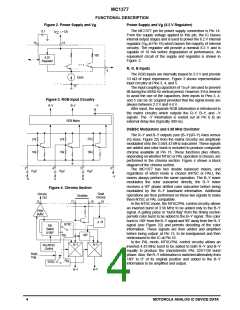
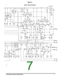
RGB Matrix
DSBSC Modulators and 3.58 MHz Oscillator
The R–Y and B–Y outputs (see (B–Y)/(R–Y) Axes versus
I/Q Axes, Figure 22) from the matrix circuitry are amplitude
modulated onto the 3.58/4.43 MHz subcarrier. These signals
are added and color burst is included to produce composite
chroma available at Pin 13. These functions plus others,
depending on whether NTSC or PAL operation is chosen, are
performed in the chroma section. Figure 4 shows a block
diagram of the chroma section.
The MC1377 has two double balanced mixers, and
regardless of which mode is chosen (NTSC or PAL), the
mixers always perform the same operation. The B–Y mixer
modulates the color subcarrier directly, the R–Y mixer
receives a 90° phase shifted color subcarrier before being
modulated by the R–Y baseband information. Additional
operations are then performed on these two signals to make
them NTSC or PAL compatible.
27k
18k
27k
18k
27k
18k
3
4
5
6
15µF
15µF
15µF
–Y
R
G
B
Figure 4. Chroma Section
Quad
Decoup
Chroma
Out
13
Oscillator
17
18
19
In the NTSC mode, the NTSC/PAL control circuitry allows
an inverted burst of 3.58 MHz to be added only to the B–Y
signal. A gating pulse or “burst flag” from the timing section
permits color burst to be added to the B–Y signal. This color
burst is 180° from the B–Y signal and 90° away from the R–Y
signal (see Figure 22) and permits decoding of the color
information. These signals are then added and amplified
before being output, at Pin 13, to be bandpassed and then
reintroduced to the IC at Pin 10.
Amp/
Buffer
∆ Θ
NTSC
PAL
Switch
0/180
°
+90°
PAL
In the PAL mode, NTSC/PAL control circuitry allows an
inverted 4.43 MHz burst to be added to both R–Y and B–Y
equally to produce the characteristic PAL 225°/135 burst
phase. Also, the R–Y information is switched alternately from
180° to 0° of its original position and added to the B–Y
information to be amplified and output.
B–Y
B–Y
R–Y
PAL/NTSC
Control
Burst
Flag
PAL
NTSC
R–Y
4
MOTOROLA ANALOG IC DEVICE DATA

 MOTOROLA [ MOTOROLA ]