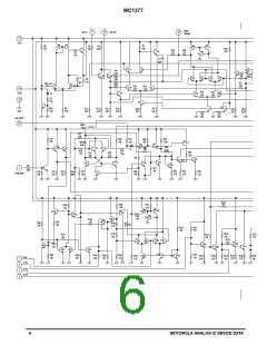
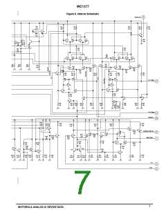
MC1377
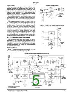
Color Reference Oscillator/Buffer
extra coupling capacitor of 50 pF from the external source to
Pin 17 was adequate with the experimentation attempted.
As stated earlier in the general description, there is an
on–board common collector Colpitts color reference
oscillator with the transistor base at Pin 17 and the emitter at
Pin 18. When used with a common low–cost TV crystal and
Voltage Controlled 90°
The oscillator drives the (B–Y) modulator and a voltage
controlled phase shifter which produces an oscillator phase
of 90° ± 5° at the (R–Y) modulator. In most situations, the
result of an error of 5° is very subtle to all but the most expert
eye. However, if it is necessary to adjust the angle to better
accuracy, the circuit shown in Figure 11 can be used.
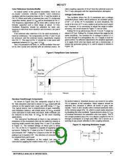
Pulling Pin 19 up will increase the (R–Y) to (B–Y) angle by
about 0.25°/µA. Pulling Pin 19 down reduces the angle by the
same sensitivity. The nominal Pin 19 voltage is about 6.3 V,
so even though it is unregulated, the 12 V supply is best for
good control. For effective adjustment, the simplest approach
is to apply RGB color bar inputs and use a vectorscope. A
simple bar generator giving R, G, and B outputs is shown in
Figure 26.
capacitive divider, about 0.6 V will be developed at Pin 17.
pp
The frequency adjustment can be done with a series 30 pF
trimmer capacitor over a total range of about 1.0 kHz.
Oscillator frequency should be adjusted for each unit,
keeping in mind that most monitors and receivers can pull in
1200 Hz.
If an external color reference is to be used exclusively, it
must be continuous. The components on Pins 17 and 18 can
be removed, and the external source capacitively coupled
into Pin 17. The input at Pin 17 should be a sine wave with
amplitude between 0.5 V and 1.0 V
.
pp pp
Also, it is possible to do both; i.e., let the oscillator “free run”
on its own crystal and override with an external source. An
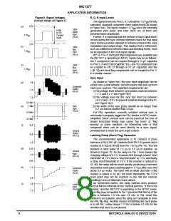
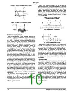
Figure 9. Ramp/Burst Gate Generator
5.0
Burst Stop
Burst Start
1.3
1.0
0
Sync
(Pin 2)
Time (µs)
0
5.5 8.5
50
63.5
Residual Feedthrough Components
As shown in Figure 9(d), the composite output at Pin 9
for fully saturated color bars is about 2.6 V , output with full
for perfect balance. Standard devices are tested to be within
5% of balance at full saturation. Black balance should be
adjusted first, because it affects all levels of gray scale
equally. There is also usually some residual baseband video
at the chroma output (Pin 13), which is most easily observed
pp
chroma on the largest bars (cyan and red) being 1.7 V
.
pp
The typical device, due to imperfections in gain, matrixing,
and modulator balance, will exhibit about 20 mV residual
pp
by disabling the color oscillator. Typical devices show 0.4 V
color subcarrier in both white and black. Both residuals can
pp
of residual luminance for saturated color bar inputs. This is
not a major problem since Pin 13 is always coupled to Pin 10
through a bandpass or a high pass filter, but it serves as a
warning to pay proper attention to the coupling network.
be reduced to less than 10 mV
applications.
for the more exacting
pp
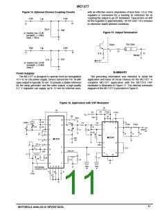
The subcarrier feedthrough in black is due primarily to
imbalance in the modulators and can be nulled by sinking or
sourcing small currents into clamp Pins 11 and 12 as shown
in Figure 12. The nominal voltage on these pins is about
4.0 Vdc, so the 8.2 V regulator is capable of supplying a pull
up source. Pulling Pin 11 down is in the 0° direction, pulling it
up is towards 180°. Pulling Pin 12 down is in the 90° direction,
pulling it up is towards 270°. Any direction of correction may
be required from part to part.
Figure 10. Adjusting Modulator Angle
12Vdc
220k
19
0.01
10k
µF
White carrier imbalance at the output can only be
corrected by juggling the relative levels of R, G, and B inputs
9
MOTOROLA ANALOG IC DEVICE DATA

 MOTOROLA [ MOTOROLA ]