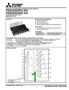
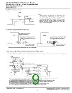
< Dual-In-Line Package Intelligent Power Module >
PSS20S92F6-AG, PSS20S92E6-AG
TRANSFER MOLDING TYPE
INSULATED TYPE
ELECTRICAL CHARACTERISTICS (Tj = 25°C, unless otherwise noted)
INVERTER PART
Limits
Typ.
1.65
1.80
0.90
2.50
1.15
0.50
1.25
0.15
0.30
-
Symbol
VCE(sat)
Parameter
Condition
IC= 20A, Tj= 25°C
Unit
V
Min.
Max.
2.00
2.15
1.10
3.00
1.55
0.80
1.75
0.30
-
-
Collector-emitter saturation
voltage
VD=VDB = 15V, VIN= 5V
VIN= 0V, -IC= 20A
IC= 20A, Tj= 125°C
IC=2.0A, Tj= 25°C
-
-
VEC
ton
FWDi forward voltage
-
V
0.75
μs
μs
μs
μs
μs
tC(on)
toff
tC(off)
trr
-
-
-
-
-
-
V
CC= 300V, VD= VDB= 15V
Switching times
IC= 20A, Tj= 125°C, VIN= 0↔5V
Inductive Load (upper-lower arm)
VCE=VCES
Tj= 25°C
1
Collector-emitter cut-off
current
ICES
mA
Tj= 125°C
-
10
CONTROL (PROTECTION) PART
Symbol Parameter
Limits
Condition
Unit
mA
Min.
-
Typ.
Max.
2.80
2.80
0.10
0.10
0.505
12.0
12.0
12.5
13.0
2.91
1.39
140
-
VD=15V, VIN=0V
VD=15V, VIN=5V
-
ID
Total of VP1-VNC, VN1-VNC
Each part of VUFB-U,
-
-
-
Circuit current
VD=VDB=15V, VIN=0V
VD=VDB=15V, VIN=5V
-
IDB
V
VFB-V, VWFB-W
-
-
(Note 3)
VSC(ref)
UVDBt
UVDBr
UVDt
Short circuit trip level
VD = 15V
0.455
7.0
7.0
10.3
10.8
2.63
0.88
100
-
0.480
10.0
10.0
-
V
V
Trip level
P-side Control supply
under-voltage protection(UV)
Reset level
V
Tj ≤125°C
Trip level
V
N-side Control supply
under-voltage protection(UV)
UVDr
Reset level
-
V
2.77
1.13
120
10
V
LVIC Temperature=90°C
LVIC Temperature=25°C
Trip level
Temperature Output
(PSS**S92F6-AG)
VOT
Pull down R=5kΩ (Note 4)
V
OTt
VD = 15V
°C
°C
V
Over temperature protection
(OT, PSS**S92E6-AG) (Note5)
OTrh
VFOH
VFOL
tFO
Detect LVIC temperature
Hysteresis of trip-reset
VSC = 0V, FO terminal pulled up to 5V by 10kΩ
4.9
-
-
-
Fault output voltage
VSC = 1V, IFO = 1mA
-
0.95
-
V
(Note 6)
Fault output pulse width
Input current
20
-
μs
mA
IIN
VIN = 5V
0.70
-
0.80
1.00
2.10
1.30
1.50
2.60
-
Vth(on)
Vth(off)
ON threshold voltage
OFF threshold voltage
ON/OFF threshold
hysteresis voltage
Applied between UP, VP, WP, UN, VN, WN-VNC
V
Vth(hys)
0.35
0.65
-
IF=10mA including voltage drop by limiting resistor
Included in bootstrap Di
(Note 7)
VF
R
Bootstrap Di forward voltage
1.1
80
1.7
2.3
V
100
120
Ω
Built-in limiting resistance
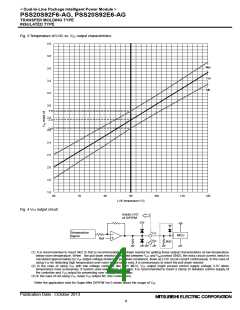
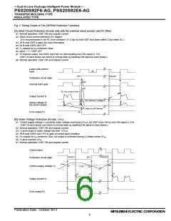
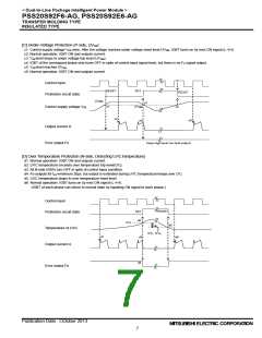
Note 3 : SC protection works only for N-side IGBT. Please select the external shunt resistance such that the SC trip-level is less than 1.7 times of the current rating.
Note 4 : DIPIPM don't shutdown IGBTs and output fault signal automatically when temperature rises excessively. When temperature exceeds the protective level that
user defined, controller (MCU) should stop the DIPIPM. Temperature of LVIC vs. VOT output characteristics is described in Fig. 3.
5 : When the LVIC temperature exceeds OT trip temperature level(OTt), OT protection works and Fo outputs. In that case if the heat sink dropped off or fixed
loosely, don't reuse that DIPIPM. (There is a possibility that junction temperature of power chips exceeded maximum Tj(150°C).
6 : Fault signal Fo outputs when SC, UV or OT protection works. Fo pulse width is different for each protection modes. At SC failure, Fo pulse width is a fixed
width (=minimum 20μs), but at UV or OT failure, Fo outputs continuously until recovering from UV or OT state. (But minimum Fo pulse width is 20μs.)
7 : The characteristics of bootstrap Di is described in Fig.2.
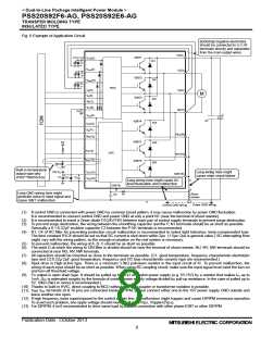
Fig. 2 Characteristics of bootstrap Di VF-IF curve (@Ta=25°C) including voltage drop by limiting resistor (Right chart is enlarged chart.)
160
140
120
30
25
20
15
10
5
100
80
60
40
20
0
0
0
1 2 3 4 5 6 7 8 9 10 11 12 13 14 15
0.0
0.5
1.0
1.5
2.0
2.5
3.0
3.5
VF [V]
VF [V]
Publication Date : October 2013
3

 MITSUBISHI [ Mitsubishi Group ]