< Dual-In-Line Package Intelligent Power Module >
PSS20S92F6-AG, PSS20S92E6-AG
TRANSFER MOLDING TYPE
INSULATED TYPE
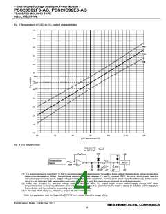
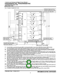
Fig. 7 MCU I/O Interface Circuit
5V line
Note)
Design for input RC filter depends on PWM control scheme used
in the application and wiring impedance of the printed circuit board.
DIPIPM input signal interface integrates minimum 3.3kΩ
10kΩ
DIPIPM
a
pull-down resistor. Therefore, when inserting RC filter, it is
necessary to satisfy turn-on threshold voltage requirement.
Fo output is open drain type. It should be pulled up to control
power supply (e.g. 5V, 15V) with a resistor that makes Fo sink
current IFo 1mA or less. In the case of pulled up to 5V supply, 10kΩ
(5kΩ or more) is recommended.
UP,VP,WP,UN,VN,WN
MCU
3.3kΩ(min)
Fo
VNC(Logic)
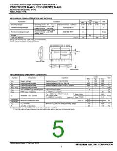
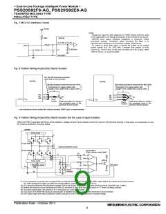
Fig. 8 Pattern Wiring Around the Shunt Resistor
NU, NV, NW should be connected
each other at near terminals.
DIPIPM
DIPIPM
Wiring Inductance should be less than 10nH.
Each wiring Inductance should be less than 10nH.
Inductance of a copper pattern with
Inductance of a copper pattern with
length=17mm, width=3mm is about 10nH.
length=17mm, width=3mm is about 10nH.
NU
NV
NW
N1
NU
NV
NW
N1
VNC
Shunt
resistor
VNC
GND wiring from VNC should
be connected close to the
terminal of shunt resistor.
GND wiring from VNC should
be connected close to the
terminal of shunt resistor.
Shunt
resistors
Low inductance shunt resistor like surface mounted (SMD) type is recommended.
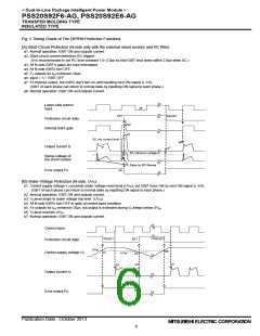
Fig. 9 Pattern Wiring Around the Shunt Resistor (for the case of open emitter)
When DIPIPM is operated with three shunt resistors, voltage of each shunt resistor cannot be input to CIN terminal directly. In that case, it is necessary to use
the external protection circuit as below.
DIPIPM
Drive circuit
P
P-side IGBT
U
V
W
External protection circuit
Comparators
N-side IGBT
(Open collector output type)
R
f
C
B
-
5V
NW
NV
NU
C
f
Vref
+
Drive circuit
-
D
OR output
Protection circuit
CIN
+
Vref
Vref
VNC
-
Shunt
resistors
A
+
N1
(1) It is necessary to set the time constant RfCf of external comparator input so that IGBT stops within 2μs when short circuit occurs.
SC interrupting time might vary with the wiring pattern, comparator speed and so on.
(2) It is recommended for the threshold voltage Vref to set to the same rating of short circuit trip level (Vsc(ref): typ. 0.48V).
(3) Select the external shunt resistance so that SC trip-level is less than specified value (=1.7 times of rating current).
(4) To avoid malfunction, the wiring A, B, C should be as short as possible.
(5) The point D at which the wiring to comparator is divided should be close to the terminal of shunt resistor.
(6) OR output high level when protection works should be over 0.505V (=maximum Vsc(ref) rating).
Publication Date : October 2013
9

 MITSUBISHI [ Mitsubishi Group ]