< Dual-In-Line Package Intelligent Power Module >
PSS20S92F6-AG, PSS20S92E6-AG
TRANSFER MOLDING TYPE
INSULATED TYPE
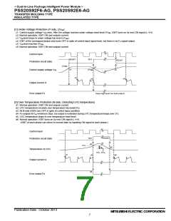
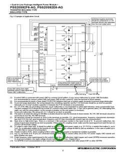
Fig. 6 Example of Application Circuit
Bootstrap negative electrodes
should be connected to U,V,W
terminals directly and separated
from the main output wires
P(24)
U(23)
IGBT1
C1
D1C2
VUFB(2)
VVFB(3)
VWFB(4)
Di1
Di2
+
+
+
IGBT2
IGBT3
HVIC
UP(5)
VP(6)
WP(7)
VP1(8)
V(22)
M
Di3
W(21)
C2
+
VNC(9)
C3
IGBT4
Di4
Di5
Di6
UN(10)
VN(11)
WN(12)
NU(20)
NV(19)
NW(18)
IGBT5
IGBT6
5V
Fo(14)
LVIC
VOT(17)
5kΩ
Built-in temperature
output type only
(PSS**S92F6-AG)
15V VD
VN1(13)
VNC(16)
Long wiring here might
cause short circuit failure
+
C1
D1
C2
C
D
Long wiring here might cause SC
level fluctuation and malfunction.
CIN(15)
B
Long GND wiring here might
generate noise to input signal and
cause IGBT malfunction.
R1
Shunt
resistor
C4
A
N1
Power GND wiring
Control GND wiring
(1) If control GND is connected with power GND by common broad pattern, it may cause malfunction by power GND fluctuation.
It is recommended to connect control GND and power GND at only a point N1 (near the terminal of shunt resistor).
(2) It is recommended to insert a Zener diode D1(24V/1W) between each pair of control supply terminals to prevent surge destruction.
(3) To prevent surge destruction, the wiring between the smoothing capacitor and the P, N1 terminals should be as short as possible.
Generally a 0.1-0.22μF snubber capacitor C3 between the P-N1 terminals is recommended.
(4) R1, C4 of RC filter for preventing protection circuit malfunction is recommended to select tight tolerance, temp-compensated type.
The time constant R1C4 should be set so that SC current is shut down within 2μs. (1.5μs~2μs is general value.) SC interrupting time
might vary with the wiring pattern, so the enough evaluation on the real system is necessary.
(5) To prevent malfunction, the wiring of A, B, C should be as short as possible.
(6) The point D at which the wiring to CIN filter is divided should be near the terminal of shunt resistor. NU, NV, NW terminals should be
connected at near NU, NV, NW terminals.
(7) All capacitors should be mounted as close to the terminals as possible. (C1: good temperature, frequency characteristic electrolytic
type and C2:0.22μ-2μF, good temperature, frequency and DC bias characteristic ceramic type are recommended.)
(8) Input drive is High-active type. There is a minimum 3.3kΩ pull-down resistor in the input circuit of IC. To prevent malfunction, the
wiring of each input should be as short as possible. When using RC coupling circuit, make sure the input signal level meet the turn-on
and turn-off threshold voltage.
(9) Fo output is open drain type. It should be pulled up to MCU or control power supply (e.g. 5V,15V) by a resistor that makes IFo up to
1mA. (IFO is estimated roughly by the formula of control power supply voltage divided by pull-up resistance. In the case of pulled up to
5V, 10kΩ (5kΩ or more) is recommended.)
(10) Thanks to built-in HVIC, direct coupling to MCU without any opto-coupler or transformer isolation is possible.
(11) Two VNC terminals (9 & 16 pin) are connected inside DIPIPM, please connect either one to the 15V power supply GND outside and
leave another one open.
(12) If high frequency noise superimposed to the control supply line, IC malfunction might happen and cause DIPIPM erroneous operation.
To avoid such problem, line ripple voltage should meet dV/dt ≤+/-1V/μs, Vripple≤2Vp-p.
(13) For DIPIPM, it isn't recommended to drive same load by parallel connection with other phase IGBT or other DIPIPM.
Publication Date : October 2013
8

 MITSUBISHI [ Mitsubishi Group ]