MITSUBISHI MICROCOMPUTERS
3827 Group
SINGLE-CHIP 8-BIT CMOS MICROCOMPUTER
Timer 1,Timer 2,Timer 3
Timer 1, timer 2, and timer 3 are 8-bit timers. The count source for
each timer can be selected by timer 123 mode register. The timer
latch value is not affected by a change of the count source. How-
ever, because changing the count source may cause an
inadvertent count down of the timer. Therefore, rewrite the value of
timer whenever the count source is changed.
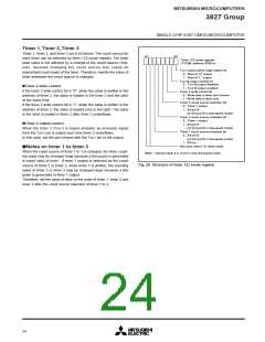
b7
b0
Timer 123 mode register
(T123M :address 002916)
TOUT output active edge switch bit
0 : Start at “H” output
1 : Start at “L” output
TOUT/φ output control bit
0 : TOUT/φ output disabled
1 : TOUT/φ output enabled
Timer 2 write control bit
0 : Write data in latch and counter
1 : Write data in latch only
Timer 2 count source selection bit
0 : Timer 1 output
●Timer 2 write control
If the timer 2 write control bit is “0”, when the value is written in the
address of timer 2, the value is loaded in the timer 2 and the latch
at the same time.
If the timer 2 write control bit is “1”, when the value is written in the
address of timer 2, the value is loaded only in the latch. The value
in the latch is loaded in timer 2 after timer 2 underflows.
1 : f(XIN)/16
(or f(XCIN)/16 in low-speed mode)
Timer 3 count source selection bit
0 : Timer 1 output
●Timer 2 output control
1 : f(XIN)/16
(or f(XCIN)/16 in low-speed mode)
Timer 1 count source selection bit
0 : f(XIN)/16
(or f(XCIN)/16 in low-speed mode)
1 : f(XCIN)
When the timer 2 (TOUT) is output enabled, an inversion signal
from the TOUT pin is output each time timer 2 underflows.
In this case, set the port shared with the TOUT pin to the output.
Not used (return “0” when read)
■Notes on timer 1 to timer 3
When the count source of timer 1 to 3 is changed, the timer count-
ing value may be changed large because a thin pulse is generated
in count input of timer . If timer 1 output is selected as the count
source of timer 2 or timer 3, when timer 1 is written, the counting
value of timer 2 or timer 3 may be changed large because a thin
pulse is generated in timer 1 output.
Note : Internal clock φ is XCIN/2 in the low-speed mode.
Fig. 20 Structure of timer 123 mode register
Therefore, set the value of timer in the order of timer 1, timer 2 and
timer 3 after the count source selection of timer 1 to 3.
24

 MITSUBISHI [ Mitsubishi Group ]