MITSUBISHI MICROCOMPUTERS
3827 Group
SINGLE-CHIP 8-BIT CMOS MICROCOMPUTER
responding to that timer is set to “1”.
TIMERS
Read and write operation on 16-bit timer must be performed for
both high and low-order bytes. When reading a 16-bit timer, read
the high-order byte first. When writing to a 16-bit timer, write the
low-order byte first. The 16-bit timer cannot perform the correct op-
eration when reading during the write operation, or when writing
during the read operation.
The 3827 group has five timers: timer X, timer Y, timer 1, timer 2,
and timer 3. Timer X and timer Y are 16-bit timers, and timer 1,
timer 2, and timer 3 are 8-bit timers.
All timers are down count timers. When the timer reaches “0016”,
an underflow occurs at the next count pulse and the correspond-
ing timer latch is reloaded into the timer and the count is
continued. When a timer underflows, the interrupt request bit cor-
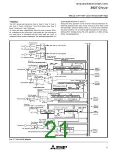
Real time port
control bit “1”
Data bus
Q D
P52 data for real time port
P52
Latch
“0”
P52 direction register
P52 latch
Real time port
control bit “1”
Q D
P53 data for real time port
P53
Real time port
control bit “0”
“0”
Latch
P53 direction register
Timer X mode register
write signal
P53 latch
“1”
f(XIN)/16
(f(XIN)/16 in low-speed mode✽)
Timer X stop
control bit
Timer X write
control bit
Timer X operat-
CNTR0 active
ing mode bits
edge switch bit
Timer X (low) latch (8)
Timer X (high) latch (8)
“00”,“01”,“11”
Timer X
interrupt
request
“0”
P54/CNTR0
Timer X (low) (8)
Timer X (high) (8)
“10”
“1”
Pulse width
measurement
CNTR0
interrupt
request
mode
CNTR0 active
edge switch bit
Pulse output mode
“0”
“1”
S
Q
Q
Timer Y operating mode bit
“00”,“01”,“10”
T
CNTR1
interrupt
request
P54 direction register
Pulse width HL continuously measurement mode
P54 latch
Pulse output mode
f(XIN)/16
Rising edge detection
“11”
Period
measurement mode
Falling edge detection
(f(XCIN)✕16 in φ = XCIN divided by 2)
Timer Y stop
control bit
Timer Y (low) latch (8)
CNTR1 active
edge switch bit
“0”
Timer Y (high) latch (8)
Timer Y (high) (8)
“00”,“01”,“11”
Timer Y
interrupt
request
P55/CNTR1
Timer Y (low) (8)
“10” Timer Y operating
mode bit
“1”
f(XIN)/16
Timer 1
interrupt
request
(f(XCIN)/16 in φ = XCIN divided by 2)
Timer 1 count source
selection bit
Timer 2 write
control bit
Timer 2 count source
selection bit
“0”
Timer 1 latch (8)
Timer 2 latch (8)
“0”
Timer 2
interrupt
request
Timer 1 (8)
XCIN
Timer 2 (8)
“1”
“1”
f(XIN)/16
(f(XCIN)✕16 in φ=XCIN divided by 2)
TOUT output
TOUT output
control bit
active edge
switch bit
“0”
TOUT output
control bit
S
Q
P43/φ/TOUT
T
“1”
P43 latch
Q
P43 direction register
Timer 3 latch (8)
Timer 3 (8)
“0”
“1”
Timer 3
interrupt
request
f(XIN)/16(f(XCIN)/16 in low-speed mode✽)
Timer 3 count
source selection bit
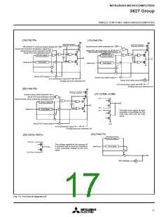
Fig. 17 Timer block diagram
21

 MITSUBISHI [ Mitsubishi Group ]