MITSUBISHI MICROCOMPUTERS
3827 Group
SINGLE-CHIP 8-BIT CMOS MICROCOMPUTER
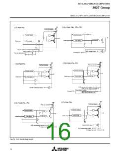
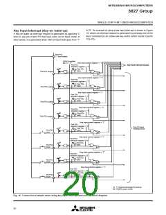
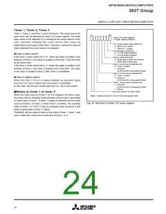
to “0”. An example of using a key input interrupt is shown in Figure
16, where an interrupt request is generated by pressing one of the
keys consisted as an active-low key matrix which inputs to ports
P20–P23.
Key Input Interrupt (Key-on wake-up)
A Key-on wake up interrupt request is generated by applying “L”
level to any pin of port P2 that have been set to input mode. In
other words, it is generated when AND of input level goes from “1”
Port PXx
“L” level output
PULLA register
Bit 2 = “1”
Key input control register = “1”
Port P27
direction register = “1”
Key input interrupt request
✽
✽
✽
✽
✽✽
Port P27
latch
Port P27 output
Key input control register = “1”
Port P26
direction register = “1”
✽✽
Port P26
latch
Port P26 output
Key input control register = “1”
Port P25
direction register = “1”
✽✽
Port P25
latch
Port P25 output
Key input control register = “1”
Port P24
direction register = “1”
✽✽
Port P24
latch
Port P24 output
Key input control register = “1”
Port P23
direction register = “0”
Port P2 input
reading circuit
✽
✽
✽✽
Port P23
latch
Port P23
input
Key input control register = “1”
direction register = “0”
Port P22
✽✽
Port P22
latch
Port P22
input
Key input control register = “1”
Port P21
direction register = “0”
✽
✽
✽✽
Port P21
latch
Port P21
input
Key input control register = “1”
Port P20
direction register = “0”
✽✽
Port P20
latch
Port P20
input
✽
P-channel transistor for pull-up
✽✽ CMOS output buffer
Fig. 16 Connection example when using key input interrupt and port P2 block diagram
20

 MITSUBISHI [ Mitsubishi Group ]