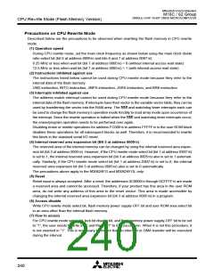
Mitsubishi microcomputers
M16C / 62 Group
SINGLE-CHIP 16-BIT CMOS MICROCOMPUTER
CPU Rewrite Mode (Flash Memory Version)
Erase All Unlock Blocks Command (A716/D016)
By writing the command code “A716” in the first bus cycle and the confirmation command code “D016”
in the second bus cycle that follows, the system starts erasing blocks successively.
Whether the erase all unlock blocks command is terminated can be confirmed by reading the status
register or the flash memory control register 0, in the same way as for block erase. Also, the status
register can be read out to know the result of the auto erase operation.
When the lock bit disable bit of the flash memory control register 0 = 1, all blocks are erased no matter
how the lock bit is set. On the other hand, when the lock bit disable bit = 0, the function of the lock bit
is effective and only nonlocked blocks (where lock bit data = 1) are erased.
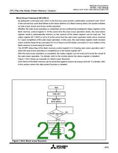
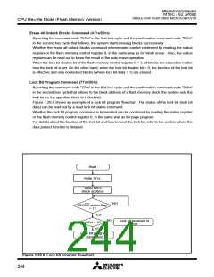
Lock Bit Program Command (7716/D016)
By writing the command code “7716” in the first bus cycle and the confirmation command code “D016”
in the second bus cycle that follows to the block address of a flash memory block, the system sets the
lock bit for the specified block to 0 (locked).
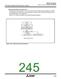
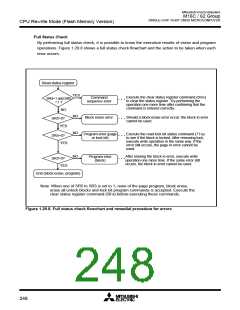
Figure 1.29.6 shows an example of a lock bit program flowchart. The status of the lock bit (lock bit
data) can be read out by a read lock bit status command.
Whether the lock bit program command is terminated can be confirmed by reading the status register
or the flash memory control register 0, in the same way as for page program.
For details about the function of the lock bit and how to reset the lock bit, refer to the section where the
data protect function is detailed.
Start
Write 7716
Write D016
block address
NO
RY/BY status flag
= 1?
YES
NO
Lock bit program in
error
SR4 = 0?
YES
Lock bit program
completed
Figure 1.29.6. Lock bit program flowchart
244

 MITSUBISHI [ Mitsubishi Group ]