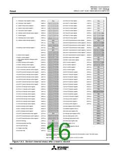
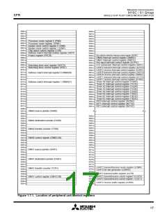
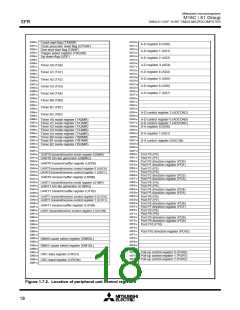
Mitsubishi microcomputers
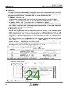
M16C / 61 Group
SINGLE-CHIP 16-BIT CMOS MICROCOMPUTER
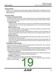
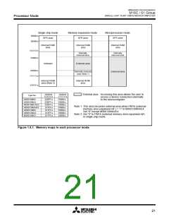
Processor Mode
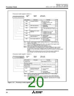
Processor mode register 0 (Note 1)
Symbol
PM0
Address
000416
When reset
0016 (Note 2)
b7 b6 b5 b4 b3 b2 b1 b0
R W
Bit symbol
Bit name
Function
b1 b0
PM00
Processor mode bit
0 0: Single-chip mode
0 1: Memory expansion mode
1 0: Inhibited
1 1: Microprocessor mode
PM01
PM02
0 : RD,BHE,WR
1 : RD,WRH,WRL
R/W mode select bit
Software reset bit
PM03
PM04
The device is reset when this bit is set
to “1”. The value of this bit is “0” when
read.
b5 b4
Multiplexed bus space
select bit
0 0 : Multiplexed bus is not used
0 1 : Allocated to CS2 space
1 0 : Allocated to CS1 space
1 1 : Allocated to entire space (Note4)
PM05
PM06
0 : Address output
1 : Port function
(Address is not output)
Port P40 to P43 function
select bit (Note 3)
0 : BCLK is output
1 : BCLK is not output
(Pin is left floating)
PM07
BCLK output disable bit
Note 1: Set bit 1 of the protect register (address 000A16) to “1” when writing new
values to this register.
Note 2: If the VCC voltage is applied to the CNVSS, the value of this register when
reset is 0316. (PM00 and PM01 both are set to “1”.)
Note 3: Valid in microprocessor and memory expansion modes.
Note 4: If the entire space is of multiplexed bus in memory expansion mode, choose
an 8-bit width.The processor operates using the separate bus after reset is
revoked, so the entire space multiplexed bus cannot be chosen in microprocessor
mode.
The higher-order address becomes a port if the entire space multiplexed
bus is chosen, so only 256 bytes can be used in each chip select.
Processor mode register 1 (Note 1)
b7 b6 b5 b4 b3 b2 b1 b0
Symbol
PM1
Address
000516
When reset
00XXXXX0
2
0
0
0
0
R W
Bit symbol
Reserved bit
Bit name
Function
Must always be set to “0”
Nothing is assigned.
In an attempt to write to these bits, write “0”. The value, if read, turns out to be
indeterminate.
Must always be set to “0”
Reserved bit
PM16
External memory area
expansion bit (Note 2)
0 : Do not expand
1 : Expand
PM17
0 : No wait state
1 : Wait state inserted
Wait bit
Note 1: Set bit 1 of the protect register (address 000A16) to “1” when writing
new values to this register.
Note 2: When this bit is set to “1” in memory expansion mode, M30612M4A/E4
provides the means of using part of internal reserved area as an external
area. Set this bit to “0” except M30612M4A/E4. Set this bit to “0” in single
chip mode.
Figure 1.8.1. Processor mode register 0 and 1
20

 MITSUBISHI [ Mitsubishi Group ]