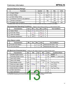
Preliminary Information
MT93L16
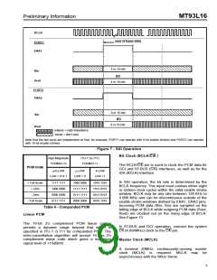
BCLK
start of frame (SSI)
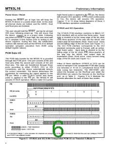
PORT1
ENA1
8 or 16 bits
Rin
EC
Sout
8 or 16 bits
PORT2
ENA2
8 or 16 bits
Sin
EC
8 or 16 bits
Rout
outputs = High impedance
inputs = don’t care
Note that the two ports are independent so that, for example, PORT1 can operate with 8-bit enable strobes and PORT2 can operate
with 16-bit enable strobes.
Figure 7 - SSI Operation
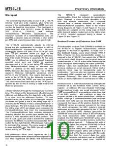
Bit Clock (BCLK/C4i )
Sign-Magnitude
FORMAT=0
ITU-T (G.711)
FORMAT=1
The BCLK/C4i pin is used to clock the PCM data for
GCI and ST-BUS (C4i) interfaces, as well as for the
SSI (BCLK) interface.
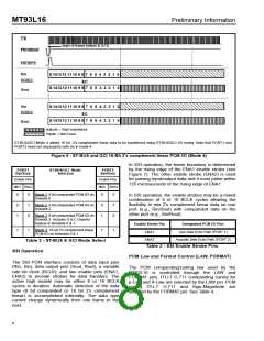
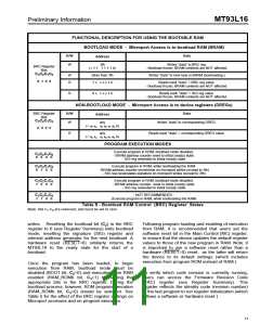
PCM Code
µ/A-LAW
µ-LAW
A-LAW
LAW = 0 or 1
LAW = 0
LAW =1
In SSI operation, the bit rate is determined by the
BCLK frequency. This input must contain either eight
or sixteen clock cycles within the valid enable strobe
window. BCLK may be any rate between 128 KHz to
4.096 MHz and can be discontinuous outside of the
enable strobe windows defined by ENA1, ENA2 pins.
Incoming PCM data (Rin, Sin) are sampled on the
falling edge of BCLK while outgoing PCM data (Sout,
Rout) are clocked out on the rising edge of BCLK.
See Figure 13.
+ Full Scale
+ Zero
1111 1111
1000 0000
0000 0000
0111 1111
1000 0000
1111 1111
0111 1111
0000 0000
1010 1010
1101 0101
0101 0101
0010 1010
- Zero
- Full Scale
Table 4 - Companded PCM
Linear PCM
The 16-bit 2’s complement PCM linear coding
permits a dynamic range beyond that which is
specified in ITU-T G.711 for companded PCM. The
echo-cancellation algorithm will accept 16 bits 2’s
complement linear code which gives a maximum
signal level of +15dBm0.
In ST-BUS and GCI operation, connect the system
C4 (4.096MHz) clock to the C4i pin.
Master Clock (MCLK)
A nominal 20MHz, continuously-running master
clock (MCLK) is required. MCLK may be
asynchronous with the 8KHz frame.
9

 MITEL [ MITEL NETWORKS CORPORATION ]