MT93L16
Preliminary Information
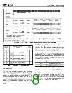
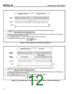
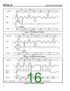
COMMAND/ADDRESS ➄
DATA INPUT/OUTPUT
A
A
A
A
A
A
X
D
D
D
D
D
D
D
D
R/W
DATA 1
0
1
2
3
4
5
0
1
2
3
4
5
6
7
➀
➁
SCLK
CS
➃
➂
➀
➁
This delay is due to internal processor timing and is equal to Tsch time. The delay is transparent to MT93L16.
The MT93L16: latches receive data on the rising edge of SCLK
outputs transmit data on the falling edge of SCLK
➂
The falling edge of CS indicates that a COMMAND/ADDRESS byte will be transmitted from the microprocessor. The subsequent
byte is always data followed by CS returning high.
A new COMMAND/ADDRESS byte may be loaded only by CS cycling high then low again.
➃
➄
The COMMAND/ADDRESS byte contains: 1 bit - Read/Write
6 bits - Addressing Data
1 bit - Unused
Figure 8 - Serial Microport Timing for Intel Mode 0
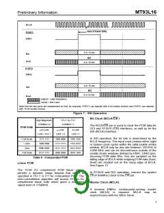
COMMAND/ADDRESS ➄
DATA INPUT
DATA 2
Receive
R/W A
A
A
A
A
A
X
D
D
D
D
D
D
D
D
5
4
3
2
1
0
7
6
5
4
3
2
1 0
DATA OUTPUT
DATA 1
Transmit
D
D
D
D
D
D
D
D
High Impedance
7
6
5
4
3
2
1 0
➀
➁
SCLK
CS
➃
➂
➀
➁
This delay is due to internal processor timing and is equal to Tsch time. The delay is transparent to MT93L16.
The MT93L16: latches receive data on the rising edge of SCLK
outputs transmit data on the falling edge of SCLK
➂
The falling edge of CS indicates that a COMMAND/ADDRESS byte will be transmitted from the microprocessor. The subsequent
byte is always data followed by CS returning high.
A new COMMAND/ADDRESS byte may be loaded only by CS cycling high then low again.
➃
➄
The COMMAND/ADDRESS byte contains: 1 bit - Read/Write
6 bits - Addressing Data
1 bit - Unused
Figure 9 - Serial Microport Timing for Motorola Mode 00 or National Microwire
12

 MITEL [ MITEL NETWORKS CORPORATION ]