Preliminary Information
MT93L16
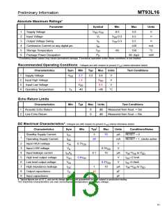
Absolute Maximum Ratings*
Parameter
Symbol
-V
Min
Max
Units
1
2
3
4
5
6
Supply Voltage
V
-0.5
5.0
5.5
5.5
±20
150
V
V
DD SS
Input Voltage
V
V
V
-0.3
i
SS
SS
Output Voltage Swing
Continuous Current on any digital pin
Storage Temperature
Package Power Dissipation
V
-0.3
V
o
I
mA
°C
i/o
T
-65
ST
P
90 (typ)
mW
D
* Exceeding these values may cause permanent damage. Functional operation under these conditions is not implied.
.
Recommended Operating Conditions - Voltages are with respect to ground (V ) unless otherwise stated
SS
Characteristics
Supply Voltage
Sym
Min
Typ
Max Units
Test Conditions
1
2
3
4
V
2.7
1.4
3.3
3.6
V
V
DD
Input High Voltage
Input Low Voltage
V
DD
V
0.4
V
SS
Operating Temperature
T
-40
+85
°C
A
Echo Return Limits
Characteristics
Acoustic Echo Return
Line Echo Return
Min
Typ
Max Units
Test Conditions
1
2
0
0
dB
dB
Measured from Rout -> Sin
Measured from Sout -> Rin
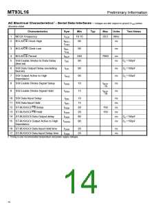
DC Electrical Characteristics*- Voltages are with respect to ground (V ) unless otherwise stated.
SS
‡
Characteristics
Sym
Min
Typ
Max
Units
Conditions/Notes
RESET = 0
RESET = 1, clocks active
Standby Supply Current:
Operating Supply Current:
Input HIGH voltage
I
I
3
70
µA
mA
V
CC
1
20
DD
2
3
4
5
6
7
8
9
V
0.7V
DD
IH
Input LOW voltage
V
0.3V
V
IL
DD
Input leakage current
High level output voltage
Low level output voltage
High impedance leakage
Output capacitance
I /I
0.1
10
µA
V
V =V to V
IH IL
IN
SS
DD
DD
V
0.8VDD
I
I
=2.5mA
OH
OH
V
0.4V
V
=5.0mA
OL
OL
OZ
DD
I
1
10
8
10
µA
pF
pF
V =V to V
IN SS
C
o
Input capacitance
C
i
‡ Typical figures are at 25°C and are for design aid only: not guaranteed and not subject to production testing.
*DC Electrical Characteristics are over recommended temperature and supply voltage.
13

 MITEL [ MITEL NETWORKS CORPORATION ]