MT93L16
Preliminary Information
C4i
start of frame (stbus & GCI)
F0i (stbus)
F0i (GCI)
Rin
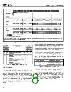
S 141312 1110 9 8 7 6 5 4 3 2 1 0
PORT1
EC
S 141312 1110 9 8 7 6 5 4 3 2 1 0
Sout
Sin
S 141312 1110 9 8 7 6 5 4 3 2 1 0
PORT2
EC
S 141312 1110 9 8 7 6 5 4 3 2 1 0
Rout
outputs = High impedance
inputs = don’t care
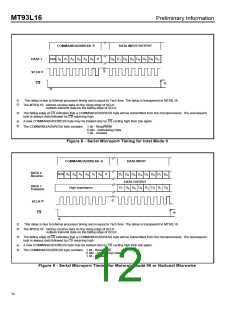
ST-BUS/GCI Mode 4 allows 16 bit 2’s complement linear data to be transferred using ST-BUS/GCI I/O timing. Note that PORT1 and
PORT2 need not necessarily both be in mode 4.
Figure 6 - ST-BUS and GCI 16-Bit 2’s complement linear PCM I/O (Mode 4)
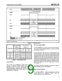
In SSI operation, the frame boundary is determined
by the rising edge of the ENA1 enable strobe (see
Figure 7). The other enable strobe (ENA2) is used
for parsing input/output data and it must pulse within
125 microseconds of the rising edge of ENA1.
PORT1
ST-BUS/GCI Mode
Selection
PORT2
Rin/Sout
Sin/Rout
Enable Pins
MD1 ENA1
Enable Pins
MD2 ENA2
0
0
1
0
1
0
Mode 1. 8 bit companded PCM I/O on
timeslot 0
0
0
1
0
1
0
In SSI operation, the enable strobes may be a mixed
combination of 8 or 16 BCLK cycles allowing the
flexibility to mix 2’s complement linear data on one
port (e.g., Rin/Sout) with companded data on the
other port (e.g., Sin/Rout).
Mode 2. 8 bit companded PCM I/O on
timeslot 2.
Mode 3. 8 bit companded PCM I/O on
timeslot 2. Includes D & C channel
bypass in timeslots 0 & 1.
Enable Strobe Pin
Designated PCM I/O Port
1
1
Mode 4. 16 bit 2’s complement linear
PCM I/O on timeslots 0 & 1.
1
1
ENA1
ENA2
Line Side Echo Path (PORT 1)
Acoustic Side Echo Path (PORT 2)
Table 2 - ST-BUS & GCI Mode Select
SSI Operation
Table 3 - SSI Enable Strobe Pins
PCM Law and Format Control (LAW, FORMAT)
The SSI PCM interface consists of data input pins
(Rin, Sin), data output pins (Sout, Rout), a variable
rate bit clock (BCLK), and two enable pins (ENA1,
ENA2) to provide strobes for data transfers. The
active high enable may be either 8 or 16 BCLK
cycles in duration. Automatic detection of the data
type (8 bit companded or 16 bit 2’s complement
linear) is accomplished internally. The data type
cannot change dynamically from one frame to the
next.
The PCM companding/coding law used by the
MT93L16 is controlled through the LAW and
FORMAT pins. ITU-T G.711 companding curves for
µ-Law and A-Law are selected by the LAW pin. PCM
coding ITU-T G.711 and Sign-Magnitude are
selected by the FORMAT pin. See Table 4.
8

 MITEL [ MITEL NETWORKS CORPORATION ]