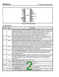
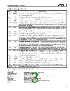
MT93L16
Preliminary Information
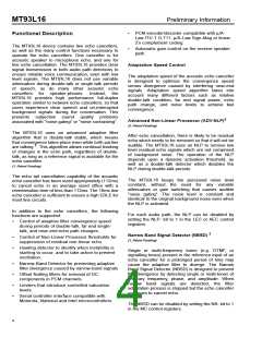
Power Down / Reset
high) frame pulse is applied to the F0i pin, the device
will assume GCI operation. If F0i is tied continuously
to Vss, the device will assume SSI operation.
Figures 11 to 13 show timing diagrams of these 3
PCM-interface operation conventions.
Holding the RESET pin at logic low will keep the
MT93L16 device in a power-down state. In this state
all internal clocks are halted, and the DATA1, Sout
and Rout pins are tristated.
ST-BUS and GCI Operation
The user should hold the RESET pin low for at least
200 msec following power-up. This will insure that
the device powers up in a proper state. Following
any return of RESET to logic high, the user must wait
for 8 complete 8 KHz frames prior to writing to the
device registers. During this time, the initialization
routines will execute and set the MT93L16 to default
operation (program execution from ROM using
default register values).
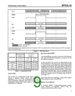
The ST-BUS PCM interface conforms to Mitel’s ST-
BUS standard, with an active-low frame pulse. Input
data is clocked in by the rising edge of the bit clock
(C4i) three-quarters of the way into the bitcell, and
output data bit boundaries (Rout, Sout) occur every
second falling edge of the bit clock (see Figure 11.)
The GCI PCM interface corresponds to the GCI
standard commonly used in Europe, with an active-
high frame pulse. Input data is clocked in by the
falling edge of the bit clock (C4i) three-quarters of
the way into the bitcell, and output data bit
boundaries (Rout, Sout) occur every second rising
edge of the bit clock (see Figure 12.)
PCM Data I/O
The PCM data transfer for the MT93L16 is provided
through two PCM ports. One port consists of Rin and
Sout pins while the second port consists of Sin and
Rout pins. The data are transferred through these
ports according to either ST-BUS, GCI, or SSI
conventions, and the device automatically detects
the correct convention. The device determines the
convention by monitoring the signal applied to the
F0i pin. When a valid ST-BUS (active low) frame
pulse is applied to the F0i pin, the MT93L16 will
assume ST-BUS operation. When a valid GCI (active
Either of these interfaces (STBUS or GCI) can be
used to transport 8 bit companded PCM data (using
one timeslot) or 16 bit 2’s complement linear PCM
data (using two timeslots). The MD1/ENA1 pins
select the timeslot on the Rin/Sout port while the
MD2/ENA2 pin selects the timeslot on the Sin/Rout
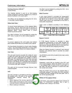
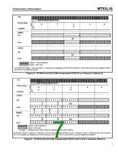
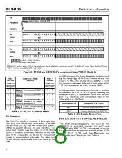
port, as in Table 2. Figures 3 to 6 illustrate the
timeslot allocation for each of these four modes.
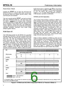
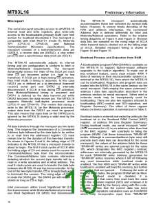
C4i
start of frame (stbus & GCI)
F0i (ST-BUS)
0
1
2
3
4
B
F0i (GCI)
PORT1
Rin
7 6 5 4 3 2 1 0
EC
Sout
7 6 5 4 3 2 1 0
PORT2
Sin
7 6 5 4 3 2 1 0
EC
7 6 5 4 3 2 1 0
Rout
outputs = High impedance
inputs = don’t care
In ST-BUS/GCI Mode 1, echo canceller I/O channels are assigned to ST-BUS/GCI timeslot 0. Note that the user can configure PORT1
and PORT2 into different modes.
Figure 3 - ST-BUS and GCI 8-Bit Companded PCM I/O on Timeslot 0 (Mode 1)
6

 MITEL [ MITEL NETWORKS CORPORATION ]