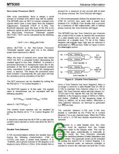
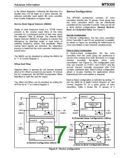
Advance Information
MT9300
Serial Data Interface Timing
Base
Addr +
Base
Addr +
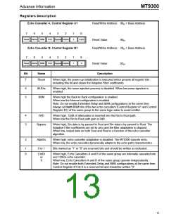
Echo Canceller A
Echo Canceller B
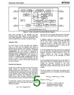
The MT9300 provides ST-BUS and GCI interface
timing. The Serial Interface clock frequency, C4i, is
4.096 MHz. The input and output data rate of the ST-
Bus and GCI bus is 2.048 Mb/s.
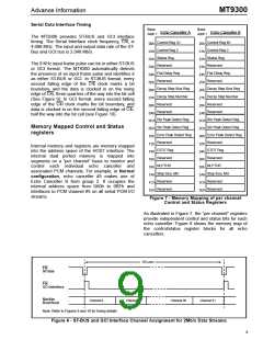
Control Reg A1
Control Reg 2
Status Reg
Control Reg B1
Control Reg 2
Status Reg
00h
01h
02h
03h
04h
05h
06h
07h
08h
0Ah
0Ch
0Eh
10h
12h
14h
16h
18h
1Ah
1Ch
1Eh
20h
21h
22h
23h
24h
25h
26h
27h
28h
2Ah
2Ch
2Eh
30h
32h
34h
36h
38h
3Ah
3Ch
3Eh
The 8 KHz input frame pulse can be in either ST-BUS
or GCI format. The MT9300 automatically detects
the presence of an input frame pulse and identifies it
as either ST-BUS or GCI. In ST-BUS format, every
second falling edge of the C4i clock marks a bit
boundary, and the data is clocked in on the rising
edge of C4i, three quarters of the way into the bit cell
(See Figure 9). In GCI format, every second falling
edge of the C4i clock marks the bit boundary, and
data is clocked in on the second falling edge of C4i,
half the way into the bit cell (see Figure 10).
Reserved
Reserved
Flat Delay Reg
Reserved
Flat Delay Reg
Reserved
Decay Step Size Reg
Decay Step Number
Reserved
Decay Step Size Reg
Decay Step Number
Reserved
Reserved
Reserved
Rin Peak Detect Reg
Sin Peak Detect Reg
Error Peak Detect Reg
Reserved
Rin Peak Detect Reg
Sin Peak Detect Reg
Error Peak Detect Reg
Reserved
Memory Mapped Control and Status
registers
Internal memory and registers are memory mapped
into the address space of the HOST interface. The
internal dual ported memory is mapped into
segments on a “per channel” basis to monitor and
control each individual echo canceller and
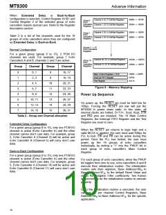
associated PCM channels. For example, in Normal
configuration, echo canceller #5 makes use of
Echo Canceller B from group 2. It occupies the
internal address space from 0A0h to 0BFh and
interfaces to PCM channel #5 on all serial PCM I/O
streams.
DTDT Reg
DTDT Reg
Reserved
Reserved
NLPTHR
NLPTHR
Step Size, MU
Reserved
Step Size, MU
Reserved
Reserved
Reserved
Figure 7 - Memory Mapping of per channel
Control and Status Registers
As illustrated in Figure 7, the “per channel” registers
provide independent control and status bits for each
echo canceller. Figure 8 shows the memory map of
the control/status register blocks for all echo
cancellers.
125 µsec
F0i
ST-Bus
F0i
GCI interface
Rin/Sin
Rout/Sout
Channel 0
Channel 1
Channel 30
Channel 31
Note: Refer to Figures 9 and 10 for timing details
Figure 6 - ST-BUS and GCI Interface Channel Assignment for 2Mb/s Data Streams
9

 MITEL [ MITEL NETWORKS CORPORATION ]